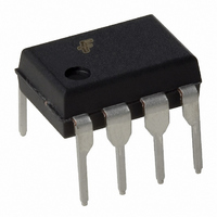
ACE1501EN Fairchild Semiconductor, ACE1501EN Datasheet - Page 13

ACE1501EN
Manufacturer Part Number
ACE1501EN
Description
IC MCU 1KBIT EEPROM 8DIP
Manufacturer
Fairchild Semiconductor
Series
ACEX® 15xxr
Datasheet
1.ACE1501EN.pdf
(33 pages)
Specifications of ACE1501EN
Core Processor
ACE1502
Core Size
8-Bit
Speed
25MHz
Peripherals
Brown-out Detect/Reset, LVD, POR, PWM, WDT
Number Of I /o
6
Program Memory Size
1KB (1K x 8)
Program Memory Type
EEPROM
Eeprom Size
64 x 8
Ram Size
64 x 8
Voltage - Supply (vcc/vdd)
1.8 V ~ 3.6 V
Oscillator Type
Internal
Operating Temperature
-40°C ~ 85°C
Package / Case
8-DIP (0.300", 7.62mm)
Lead Free Status / RoHS Status
Lead free / RoHS Compliant
Data Converters
-
Connectivity
-
ACE1501 Product Family Rev. 1.1
3.5 Memory
The ACEx microcontroller has 64 bytes of SRAM and 64 bytes
of EEPROM available for data storage. The device also has 1K
bytes of EEPROM for program storage. Software can read and
write to SRAM and data EEPROM but can only read from the
code EEPROM. While in normal mode, the code EEPROM is
protected from any writes. The code EEPROM can only be
rewritten when the device is in program mode and if the write
disable (WDIS) bit of the initialization register is not set to 1.
While in normal mode, the user can write to the data EEPROM
array by 1) polling the ready (R) flag of the SR, then 2) execut-
ing the appropriate instruction. If the R flag is 1, the data
EEPROM block is ready to perform the next write. If the R flag is
0, the data EEPROM is busy. The data EEPROM array will
reset the R flag after the completion of a write cycle. Attempts to
Figure 14. Initialization Register 1
(0) RDIS
(1) WDIS
(2) UBD
(3) LBDEN
(4) BOREN
(5) WDEN
(6) CMODE[1]
(7) CMODE[0]
4. Timer 1
Timer 1 is a versatile 16-bit timer that can operate in one of four
modes:
• Pulse Width Modulation (PWM) mode, which generates
• External Event Counter mode, which counts occurrences of
• Standard Input Capture mode, which measures the elapsed
• Difference Input Capture mode, which automatically mea-
Timer 1 contains a 16-bit timer/counter register (TMR1), a 16-bit
auto-reload/capture register (T1RA), a secondary 16-bit auto-
reload
(T1CNTRL). All register are memory-mapped for simple access
through the core with both the 16-bit registers organized as a
pair of 8-bit register bytes {TMR1HI, TMR1LO}, {T1RAHI,
T1RALO}, and {T1RBHI, T1RBLO}. Depending on the operating
mode, the timer contains an external input or output (T1) that is
multiplexed with the I/O pin G2. By default, the TMR1 is reset to
0xFFFF, T1RA/T1RB is reset to 0x0000, and T1CNTRL is reset
to 0x00.
pulses of a specified width and duty cycle
an external event
time between occurrences of external events
sures the difference between edges.
CMODE[0]
Bit 7
register
(T1RB),
CMODE[1]
Bit 6
If set, disables attempts to read the contents from the memory while in programming mode. Once this bit is
set, it is no longer possible to unset this option even though the write disable option is not enabled.
If set, disables attempts to write new contents to the memory while in programming mode
If set, the device will not allow any writes to occur in the upper block of data EEPROM (0x60-0x7F)
If set, the Low Battery Detection circuit is enabled
If set, allows a BOR to occur if Vcc falls below the voltage reference level
If set, enables the on-chip processor watchdog circuit
Clock mode select bit 1 (See Table 16)
Clock mode select bit 0 (See Table 16)
and
an
WDEN
Bit 5
8-bit
control
BOREN
Bit 4
register
13
read, write, or enter HALT/IDLE mode while the data EEPROM
is busy (R = 0) can affect the current data being written.
3.6 Initialization Registers
The ACEx microcontroller has two 8-bit wide initialization
registers. These registers are read from the memory space on
power-up to initialize certain on-chip peripherals. Figure 14
provides a detailed description of Initialization Register 1. The
Initialization Register 2 is used to trim the internal oscillator to
its appropriate frequency. This register is pre-programmed in
the factory to yield an internal instruction clock of 1MHz.
The Initialization Registers 1 and 2 can be read from and written
to during programming mode. However, re-trimming the inter-
nal oscillator (writing to the Initialization Register 2) once it has
left the factory is discouraged.
The timer can be started or stopped through the T1CNTRL reg-
ister bit T1C0. When running, the timer counts down (decre-
ments) every clock cycle. Depending on the operating mode,
the timer’s clock is either the instruction clock or a transition on
the T1 input. In addition, occurrences of timer underflow (transi-
tions from 0x0000 to 0xFFFF/T1RA/T1RB value) can either
generate an interrupt and/or toggle the T1 output pin.
Timer 1’s interrupt (TMRI1) can be enabled by interrupt enable
(T1EN) bit in the T1CNTRL register. When the timer interrupt is
enabled, depending on the operating mode, the source of the
interrupt is a timer underflow and/or a timer capture.
4.1 Timer control bits
Reading and writing to the T1CNTRL register controls the
timer’s operation. By writing to the control bits, the user can
enable or disable the timer interrupts, set the mode of operation,
and start or stop the timer. The T1CNTRL register bits are
described in Table 11 and Table 12.
LDBEN
Bit 3
Bit 2
UBD
Bit 1
WDIS
www.fairchildsemi.com
Bit 0
RDIS


