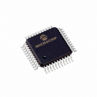
PIC16LC774/PQ Microchip Technology, PIC16LC774/PQ Datasheet - Page 7

PIC16LC774/PQ
Manufacturer Part Number
PIC16LC774/PQ
Description
IC MCU OTP 4KX14 A/D PWM 44-MQFP
Manufacturer
Microchip Technology
Series
PIC® 16Cr
Specifications of PIC16LC774/PQ
Core Processor
PIC
Core Size
8-Bit
Speed
20MHz
Connectivity
I²C, SPI, UART/USART
Peripherals
Brown-out Detect/Reset, POR, PWM, WDT
Number Of I /o
33
Program Memory Size
7KB (4K x 14)
Program Memory Type
OTP
Ram Size
256 x 8
Voltage - Supply (vcc/vdd)
2.5 V ~ 5.5 V
Data Converters
A/D 10x12b
Oscillator Type
External
Operating Temperature
0°C ~ 70°C
Package / Case
44-MQFP, 44-PQFP
Processor Series
PIC16LC
Core
PIC
Data Bus Width
8 bit
Data Ram Size
256 B
Interface Type
I2C, SPI, SSP, UART
Maximum Clock Frequency
20 MHz
Number Of Programmable I/os
33
Number Of Timers
3 bit
Operating Supply Voltage
2.5 V to 5.5 V
Maximum Operating Temperature
+ 70 C
Mounting Style
SMD/SMT
3rd Party Development Tools
52715-96, 52716-328, 52717-734
Development Tools By Supplier
ICE2000, DM163022
Minimum Operating Temperature
0 C
On-chip Adc
10 bit
Lead Free Status / RoHS Status
Lead free / RoHS Compliant
Eeprom Size
-
Lead Free Status / Rohs Status
Details
Available stocks
Company
Part Number
Manufacturer
Quantity
Price
Company:
Part Number:
PIC16LC774/PQ
Manufacturer:
Microchip Technology
Quantity:
10 000
TABLE 1-1
Pin Name
OSC1/CLKIN
OSC2/CLKOUT
MCLR/V
RA0/AN0
RA1/AN1
RA2/AN2/V
RA3/AN3/V
RA4/T0CKI
RB0/INT
RB1/SS
RB2/AN8
RB3/AN9/LVDIN
RB4
RB5
RB6
RB7
RC0/T1OSO/T1CKI
RC1/T1OSI/CCP2
RC2/CCP1
RC3/SCK/SCL
RC4/SDI/SDA
RC5/SDO
RC6/TX/CK
RC7/RX/DT
AV
AV
V
V
Legend: I = input
Note 1: This buffer is a Schmitt Trigger input when configured for the multiplexed function.
SS
DD
1999 Microchip Technology Inc.
SS
DD
2: This buffer is a Schmitt Trigger input when used in serial programming mode.
3: This buffer is a Schmitt Trigger input when configured in RC oscillator mode and a CMOS input otherwise.
PP
REF
REF
-/VRL
+/VRH
PIC16C773 PINOUT DESCRIPTION
O = output
— = Not used
SSOP,
SOIC
Pin#
DIP,
10
21
22
25
26
27
28
11
12
13
15
16
17
18
19
20
23
24
14
9
1
2
3
4
5
6
8
7
I/O/P
Type
I/O
I/O
I/O
I/O
I/O
I/O
I/O
I/O
I/O
I/O
I/O
I/O
I/O
I/O
I/O
I/O
I/O
I/O
I/O
I/O
I/O
I/P
O
P
P
P
P
I
ST/CMOS
TTL/ST
TTL/ST
TTL/ST
TTL/ST
I/O = input/output
TTL = TTL input
Buffer
Advance Information
Type
TTL
TTL
TTL
TTL
TTL
TTL
TTL
TTL
ST
ST
ST
ST
ST
ST
ST
ST
ST
ST
—
—
—
(1)
(1)
(2)
(2)
(3)
Description
Oscillator crystal input/external clock source input.
Oscillator crystal output. Connects to crystal or resonator in crystal
oscillator mode. In RC mode, the OSC2 pin outputs CLKOUT which has
1/4 the frequency of OSC1, and denotes the instruction cycle rate.
Master clear (reset) input or programming voltage input. This pin is an
active low reset to the device.
PORTA is a bi-directional I/O port.
PORTB is a bi-directional I/O port. PORTB can be software pro-
grammed for internal weak pull-up on all inputs.
PORTC is a bi-directional I/O port.
Ground reference for A/D converter
Positive supply for A/D converter
Ground reference for logic and I/O pins.
Positive supply for logic and I/O pins.
RA0 can also be analog input0
RA1 can also be analog input1
RA2 can also be analog input2 or negative analog reference voltage
input or internal voltage reference low
RA3 can also be analog input3 or positive analog reference voltage
input or internal voltage reference high
RA4 can also be the clock input to the Timer0 module. Output is
open drain type.
RB0 can also be the external interrupt pin.
RB1 can also be the SSP slave select
RB2 can also be analog input8
RB3 can also be analog input9 or the low voltage detect input
reference
Interrupt on change pin.
Interrupt on change pin.
Interrupt on change pin. Serial programming clock.
Interrupt on change pin. Serial programming data.
RC0 can also be the Timer1 oscillator output or Timer1 clock input.
RC1 can also be the Timer1 oscillator input or Capture2 input/
Compare2 output/PWM2 output.
RC2 can also be the Capture1 input/Compare1 output/PWM1
output.
RC3 can also be the synchronous serial clock input/output for both
SPI and I
RC4 can also be the SPI Data In (SPI mode) or
data I/O (I
RC5 can also be the SPI Data Out (SPI mode).
RC6 can also be the USART Asynchronous Transmit or
Synchronous Clock.
RC7 can also be the USART Asynchronous Receive or
Synchronous Data.
P = power
ST = Schmitt Trigger input
2
2
C modes.
C mode).
PIC16C77X
DS30275A-page 7


