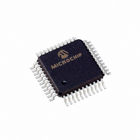
PIC16LC774/PQ Microchip Technology, PIC16LC774/PQ Datasheet - Page 119

PIC16LC774/PQ
Manufacturer Part Number
PIC16LC774/PQ
Description
IC MCU OTP 4KX14 A/D PWM 44-MQFP
Manufacturer
Microchip Technology
Series
PIC® 16Cr
Specifications of PIC16LC774/PQ
Core Processor
PIC
Core Size
8-Bit
Speed
20MHz
Connectivity
I²C, SPI, UART/USART
Peripherals
Brown-out Detect/Reset, POR, PWM, WDT
Number Of I /o
33
Program Memory Size
7KB (4K x 14)
Program Memory Type
OTP
Ram Size
256 x 8
Voltage - Supply (vcc/vdd)
2.5 V ~ 5.5 V
Data Converters
A/D 10x12b
Oscillator Type
External
Operating Temperature
0°C ~ 70°C
Package / Case
44-MQFP, 44-PQFP
Processor Series
PIC16LC
Core
PIC
Data Bus Width
8 bit
Data Ram Size
256 B
Interface Type
I2C, SPI, SSP, UART
Maximum Clock Frequency
20 MHz
Number Of Programmable I/os
33
Number Of Timers
3 bit
Operating Supply Voltage
2.5 V to 5.5 V
Maximum Operating Temperature
+ 70 C
Mounting Style
SMD/SMT
3rd Party Development Tools
52715-96, 52716-328, 52717-734
Development Tools By Supplier
ICE2000, DM163022
Minimum Operating Temperature
0 C
On-chip Adc
10 bit
Lead Free Status / RoHS Status
Lead free / RoHS Compliant
Eeprom Size
-
Lead Free Status / Rohs Status
Details
Available stocks
Company
Part Number
Manufacturer
Quantity
Price
Company:
Part Number:
PIC16LC774/PQ
Manufacturer:
Microchip Technology
Quantity:
10 000
The value that is in the ADRESH and ADRESL regis-
ters are not modified for a Power-on Reset. The
ADRESH and ADRESL registers will contain unknown
data after a Power-on Reset.
After the A/D module has been configured as desired,
the selected channel must be acquired before the con-
version is started. The analog input channels must
have their corresponding TRIS bits selected as an
input. To determine acquisition time, see
After this acquisition time has elapsed the A/D conver-
sion can be started. The following steps should be fol-
lowed for doing an A/D conversion:
11.2
11.3
The ADCON1 and TRIS registers control the operation
of the A/D port pins. The port pins that are desired as
analog inputs must have their corresponding TRIS bit
set (input). If the TRIS bit is cleared (output), the digital
output level (V
The A/D operation is independent of the state of the
CHS3:CHS0 bits and the TRIS bits.
11.3.1
The VCFG bits in the ADCON1 register configure the
A/D module reference inputs.
input can come from an internal reference (VRH) or
(VRL), an external reference (V
low reference input can come from an internal refer-
ence (VRL), an external reference (V
an external reference is chosen for the reference high
or reference low inputs, the port pin that multiplexes
the incoming external references is configured as an
analog input, regardless of the values contained in the
A/D port configuration bits (PCFG3:PCFG0).
1999 Microchip Technology Inc.
Note 1: When reading the PORTA or PORTE reg-
Note 2: Analog levels on any pin that is defined as
Configuring the A/D Module
Configuring Analog Port Pins
CONFIGURING THE REFERENCE
VOLTAGES
ister, all pins configured as analog input
channels will read as cleared (a low level).
When reading the PORTB register, all
pins configured as analog input channels
will read as set (a high level). Pins config-
ured as digital inputs, will convert an ana-
log input.
configured input will not affect the conver-
sion accuracy.
a digital input (including the ANx pins),
may cause the input buffer to consume
current that is out of the devices specifica-
tion.
OH
or V
OL
) will be converted.
Analog levels on a digitally
REF
The reference high
+), or A
REF
-), or A
Section
Advance Information
VDD
VSS
. The
11.6.
. If
After the A/D module has been configured as desired.
and the analog input channels have their correspond-
ing TRIS bits selected for port inputs, the selected
channel must be acquired before conversion is
started. The A/D conversion cycle can be initiated by
setting the GO/DONE bit. The A/D conversion begins,
and lasts for 13T
lowed for performing an A/D conversion:
1.
2.
3.
4.
5.
6.
7.
Clearing the GO/DONE bit during a conversion will
abort the current conversion. The ADRESH and
ADRESL registers WILL be updated with the partially
completed A/D conversion value. That is, the ADRESH
and ADRESL registers WILL contain the value of the
current incomplete conversion.
Note:
Configure the A/D module
• Configure analog pins / voltage reference /
• Select A/D input channel (ADCON0)
• Select A/D conversion clock (ADCON0)
• Turn on A/D module (ADCON0)
Configure A/D interrupt (if required)
• Clear ADIF bit
• Set ADIE bit
• Set PEIE bit
• Set GIE bit
Wait the required acquisition time (3T
Start conversion
• Set GO/DONE bit (ADCON0)
Wait 13T
either:
• Polling for the GO/DONE bit to be cleared
OR
• Waiting for the A/D interrupt
Read A/D Result registers (ADRESH and
ADRESL), clear ADIF if required.
For next conversion, go to step 1, step 2 or step
3 as required.
and digital I/O (ADCON1)
Do not set the ADON bit and the
GO/DONE bit in the same instruction.
Doing so will cause the GO/DONE bit to be
automatically cleared.
AD
until A/D conversion is complete, by
AD
. The following steps should be fol-
PIC16C77X
DS30275A-page 119
AD
)


