PIC16LC774/PQ Microchip Technology, PIC16LC774/PQ Datasheet - Page 190
PIC16LC774/PQ
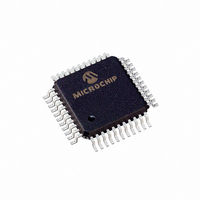
Manufacturer Part Number
PIC16LC774/PQ
Description
IC MCU OTP 4KX14 A/D PWM 44-MQFP
Manufacturer
Microchip Technology
Series
PIC® 16Cr
Specifications of PIC16LC774/PQ
Core Processor
PIC
Core Size
8-Bit
Speed
20MHz
Connectivity
I²C, SPI, UART/USART
Peripherals
Brown-out Detect/Reset, POR, PWM, WDT
Number Of I /o
33
Program Memory Size
7KB (4K x 14)
Program Memory Type
OTP
Ram Size
256 x 8
Voltage - Supply (vcc/vdd)
2.5 V ~ 5.5 V
Data Converters
A/D 10x12b
Oscillator Type
External
Operating Temperature
0°C ~ 70°C
Package / Case
44-MQFP, 44-PQFP
Processor Series
PIC16LC
Core
PIC
Data Bus Width
8 bit
Data Ram Size
256 B
Interface Type
I2C, SPI, SSP, UART
Maximum Clock Frequency
20 MHz
Number Of Programmable I/os
33
Number Of Timers
3 bit
Operating Supply Voltage
2.5 V to 5.5 V
Maximum Operating Temperature
+ 70 C
Mounting Style
SMD/SMT
3rd Party Development Tools
52715-96, 52716-328, 52717-734
Development Tools By Supplier
ICE2000, DM163022
Minimum Operating Temperature
0 C
On-chip Adc
10 bit
Lead Free Status / RoHS Status
Lead free / RoHS Compliant
Eeprom Size
-
Lead Free Status / Rohs Status
Details
Available stocks
Company
Part Number
Manufacturer
Quantity
Price
Company:

Part Number:
PIC16LC774/PQ
Manufacturer:
Microchip Technology
Quantity:
10 000


PIC16C77X
E
Errata ................................................................................... 4
External Power-on Reset Circuit ...................................... 132
F
Firmware Instructions ....................................................... 143
Flowcharts
FSR Register .......................................................... 13, 14, 15
Fuzzy Logic Dev. System ( fuzzy TECH -MP) .................. 147
G
GCE ................................................................................... 56
General Call Address Sequence ........................................ 69
General Call Address Support ........................................... 69
General Call Enable bit, GCE ............................................ 56
I
I/O Ports ............................................................................. 27
I
I
I
I
I
I
DS30275A-page 190
2
2
2
2
2
2
C ...................................................................................... 63
C Master Mode Receiver Flowchart ................................ 83
C Master Mode Reception ............................................... 82
C Master Mode Restart Condition ................................... 76
C Mode Selection ............................................................ 63
C Module
Acknowledge .............................................................. 86
Master Receiver ......................................................... 83
Master Transmit ......................................................... 80
Restart Condition ....................................................... 77
Start Condition ........................................................... 75
Stop Condition ........................................................... 88
Acknowledge Flowchart ............................................. 86
Acknowledge Sequence timing .................................. 85
Addressing ................................................................. 64
Baud Rate Generator ................................................. 73
Block Diagram ............................................................ 71
BRG Block Diagram ................................................... 73
BRG Reset due to SDA Collision ............................... 92
BRG Timing ............................................................... 73
Bus Arbitration ........................................................... 90
Bus Collision .............................................................. 90
Bus Collision timing .................................................... 90
Clock Arbitration ......................................................... 89
Clock Arbitration Timing (Master Transmit) ................ 89
Conditions to not give ACK Pulse .............................. 64
General Call Address Support ................................... 69
Master Mode .............................................................. 71
Master Mode 7-bit Reception timing .......................... 84
Master Mode Operation ............................................. 72
Master Mode Start Condition ..................................... 74
Master Mode Transmission ........................................ 79
Master Mode Transmit Sequence .............................. 72
Master Transmit Flowchart ........................................ 80
Multi-Master Communication ..................................... 90
Multi-master Mode ..................................................... 72
Operation ................................................................... 63
Repeat Start Condition timing .................................... 76
Acknowledge ...................................................... 90
Restart Condition ............................................... 93
Restart Condition Timing (Case1) ...................... 93
Restart Condition Timing (Case2) ...................... 93
Start Condition ................................................... 91
Start Condition Timing ................................. 91, 92
Stop Condition ................................................... 94
Stop Condition Timing (Case1) .......................... 94
Stop Condition Timing (Case2) .......................... 94
Transmit Timing ................................................. 90
Preliminary
I
I
ICEPIC Low-Cost PIC16CXXX In-Circuit Emulator ......... 145
ID Locations ............................................................. 127, 141
In-Circuit Serial Programming (ICSP) ...................... 127, 141
INDF .................................................................................. 15
INDF Register .............................................................. 13, 14
Indirect Addressing ............................................................ 25
Instruction Format ............................................................ 143
Instruction Set .................................................................. 143
INTCON ............................................................................. 15
INTCON Register ............................................................... 18
Inter-Integrated Circuit (I
internal sampling switch (Rss) impedence ...................... 123
Interrupt Sources ..................................................... 127, 137
Interrupts, Context Saving During .................................... 138
Interrupts, Enable Bits
2
2
C Module Address Register, SSPADD ........................... 64
C Slave Mode .................................................................. 64
Restart Condition Flowchart ...................................... 77
Slave Mode ................................................................ 64
Slave Reception ........................................................ 65
Slave Transmission ................................................... 65
SSPBUF .................................................................... 64
Start Condition Flowchart .......................................... 75
Stop Condition Flowchart ........................................... 88
Stop Condition Receive or Transmit timing ............... 87
Stop Condition timing ................................................. 87
Waveforms for 7-bit Reception .................................. 65
Waveforms for 7-bit Transmission ............................. 66
FSR Register ............................................................. 11
Summary Table ....................................................... 144
GIE Bit ....................................................................... 18
INTE Bit ..................................................................... 18
INTF Bit ..................................................................... 18
PEIE Bit ..................................................................... 18
RBIE Bit ..................................................................... 18
RBIF Bit ............................................................... 18, 30
T0IE Bit ...................................................................... 18
T0IF Bit ...................................................................... 18
Block Diagram ......................................................... 137
Capture Complete (CCP) ........................................... 48
Compare Complete (CCP) ......................................... 49
Interrupt on Change (RB7:RB4 ) ............................... 30
RB0/INT Pin, External ...................................... 7, 8, 138
TMR0 Overflow .................................................. 40, 138
TMR1 Overflow .................................................... 41, 43
TMR2 to PR2 Match .................................................. 46
TMR2 to PR2 Match (PWM) ................................ 45, 50
USART Receive/Transmit Complete ......................... 97
A/D Converter Enable (ADIE Bit) ............................... 19
CCP1 Enable (CCP1IE Bit) ................................. 19, 48
CCP2 Enable (CCP2IE Bit) ....................................... 21
Global Interrupt Enable (GIE Bit) ....................... 18, 137
Interrupt on Change (RB7:RB4) Enable
(RBIE Bit) ........................................................... 18, 138
Peripheral Interrupt Enable (PEIE Bit) ....................... 18
PSP Read/Write Enable (PSPIE Bit) ......................... 19
RB0/INT Enable (INTE Bit) ........................................ 18
SSP Enable (SSPIE Bit) ............................................ 19
TMR0 Overflow Enable (T0IE Bit) ............................. 18
TMR1 Overflow Enable (TMR1IE Bit) ........................ 19
TMR2 to PR2 Match Enable (TMR2IE Bit) ................ 19
USART Receive Enable (RCIE Bit) ........................... 19
USART Transmit Enable (TXIE Bit) ........................... 19
2
C) .............................................. 53
1999 Microchip Technology Inc.
Related parts for PIC16LC774/PQ
Image
Part Number
Description
Manufacturer
Datasheet
Request
R

Part Number:
Description:
3.5KB Flash, 128B RAM, 18 I/O, CLC, CWG, DDS, 10-bit ADC 20 QFN 4x4mm TUBE
Manufacturer:
Microchip Technology
Datasheet:

Part Number:
Description:
3.5KB Flash, 128B RAM, 18 I/O, CLC, CWG, DDS, 10-bit ADC 20 PDIP .300in TUBE
Manufacturer:
Microchip Technology
Datasheet:

Part Number:
Description:
3.5KB Flash, 128B RAM, 18 I/O, CLC, CWG, DDS, 10-bit ADC 20 SOIC .300in TUBE
Manufacturer:
Microchip Technology
Datasheet:

Part Number:
Description:
3.5KB Flash, 128B RAM, 18 I/O, CLC, CWG, DDS, 10-bit ADC 20 SSOP .209in TUBE
Manufacturer:
Microchip Technology
Datasheet:
Part Number:
Description:
3.5KB Flash, 128B RAM, 18 I/O, CLC, CWG, DDS, 10-bit ADC 20 QFN 4x4mm TUBE
Manufacturer:
Microchip Technology
Datasheet:
Part Number:
Description:
3.5KB Flash, 128B RAM, 18 I/O, CLC, CWG, DDS, 10-bit ADC 20 PDIP .300in TUBE
Manufacturer:
Microchip Technology
Datasheet:
Part Number:
Description:
3.5KB Flash, 128B RAM, 18 I/O, CLC, CWG, DDS, 10-bit ADC 20 SOIC .300in TUBE
Manufacturer:
Microchip Technology
Datasheet:
Part Number:
Description:
3.5KB Flash, 128B RAM, 18 I/O, CLC, CWG, DDS, 10-bit ADC 20 SSOP .209in TUBE
Manufacturer:
Microchip Technology
Datasheet:
Part Number:
Description:
3.5KB Flash, 128B RAM, 18 I/O, CLC, CWG, DDS, 10-bit ADC 20 QFN 4x4mm T/R
Manufacturer:
Microchip Technology
Datasheet:
Part Number:
Description:
3.5KB Flash, 128B RAM, 18 I/O, CLC, CWG, DDS, 10-bit ADC 20 SOIC .300in T/R
Manufacturer:
Microchip Technology
Datasheet:
Part Number:
Description:
3.5KB Flash, 128B RAM, 18 I/O, CLC, CWG, DDS, 10-bit ADC 20 SSOP .209in T/R
Manufacturer:
Microchip Technology
Datasheet:
Part Number:
Description:
3.5KB Flash, 128B RAM, 18 I/O, CLC, CWG, DDS, 10-bit ADC 20 QFN 4x4mm TUBE
Manufacturer:
Microchip Technology
Datasheet:
Part Number:
Description:
3.5KB Flash, 128B RAM, 18 I/O, CLC, CWG, DDS, 10-bit ADC 20 PDIP .300in TUBE
Manufacturer:
Microchip Technology
Datasheet:
Part Number:
Description:
3.5KB Flash, 128B RAM, 18 I/O, CLC, CWG, DDS, 10-bit ADC 20 SOIC .300in TUBE
Manufacturer:
Microchip Technology
Datasheet:
Part Number:
Description:
3.5KB Flash, 128B RAM, 18 I/O, CLC, CWG, DDS, 10-bit ADC 20 SSOP .209in TUBE
Manufacturer:
Microchip Technology
Datasheet: