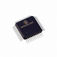
PIC16LC774/PQ Microchip Technology, PIC16LC774/PQ Datasheet - Page 49

PIC16LC774/PQ
Manufacturer Part Number
PIC16LC774/PQ
Description
IC MCU OTP 4KX14 A/D PWM 44-MQFP
Manufacturer
Microchip Technology
Series
PIC® 16Cr
Specifications of PIC16LC774/PQ
Core Processor
PIC
Core Size
8-Bit
Speed
20MHz
Connectivity
I²C, SPI, UART/USART
Peripherals
Brown-out Detect/Reset, POR, PWM, WDT
Number Of I /o
33
Program Memory Size
7KB (4K x 14)
Program Memory Type
OTP
Ram Size
256 x 8
Voltage - Supply (vcc/vdd)
2.5 V ~ 5.5 V
Data Converters
A/D 10x12b
Oscillator Type
External
Operating Temperature
0°C ~ 70°C
Package / Case
44-MQFP, 44-PQFP
Processor Series
PIC16LC
Core
PIC
Data Bus Width
8 bit
Data Ram Size
256 B
Interface Type
I2C, SPI, SSP, UART
Maximum Clock Frequency
20 MHz
Number Of Programmable I/os
33
Number Of Timers
3 bit
Operating Supply Voltage
2.5 V to 5.5 V
Maximum Operating Temperature
+ 70 C
Mounting Style
SMD/SMT
3rd Party Development Tools
52715-96, 52716-328, 52717-734
Development Tools By Supplier
ICE2000, DM163022
Minimum Operating Temperature
0 C
On-chip Adc
10 bit
Lead Free Status / RoHS Status
Lead free / RoHS Compliant
Eeprom Size
-
Lead Free Status / Rohs Status
Details
Available stocks
Company
Part Number
Manufacturer
Quantity
Price
Company:
Part Number:
PIC16LC774/PQ
Manufacturer:
Microchip Technology
Quantity:
10 000
7.2
In Compare mode, the 16-bit CCPR1 register value is
constantly compared against the TMR1 register pair
value. When a match occurs, the RC2/CCP1 pin is:
• driven High
• driven Low
• remains Unchanged
The action on the pin is based on the value of control
bits CCP1M3:CCP1M0 (CCP1CON<3:0>). At the
same time, interrupt flag bit CCP1IF is set.
FIGURE 7-3:
TABLE 7-3
Address
0Bh,8Bh,
10Bh,18Bh
0Ch
8Ch
87h
0Eh
0Fh
10h
15h
16h
17h
Legend:
Note 1:
RC2/CCP1
Pin
1999 Microchip Technology Inc.
Special event trigger will:
reset Timer1, but not set interrupt flag bit TMR1IF (PIR1<0>),
and set bit GO/DONE (ADCON0<2>)
which starts an A/D conversion
Output Enable
TRISC<2>
Compare Mode
Bits PSPIE and PSPIF are reserved on the 28-pin, always maintain these bits clear.
x = unknown, u = unchanged, - = unimplemented read as ’0’. Shaded cells are not used by Capture and Timer1.
Name
INTCON
PIR1
PIE1
TRISC
TMR1L
TMR1H
T1CON
CCPR1L
CCPR1H
CCP1CON
Q
Special Event Trigger (CCP2 only)
COMPARE MODE
OPERATION BLOCK
DIAGRAM
REGISTERS ASSOCIATED WITH CAPTURE, COMPARE, AND TIMER1
R
S
CCP1CON<3:0>
Mode Select
Output
PORTC Data Direction Register
Holding register for the Least Significant Byte of the 16-bit TMR1 register
Holding register for the Most Significant Byte of the 16-bit TMR1register
Capture/Compare/PWM register1 (LSB)
Capture/Compare/PWM register1 (MSB)
Logic
PSPIE
PSPIF
Bit 7
GIE
—
—
(PIR1<2>)
Set flag bit CCP1IF
(1)
(1)
match
ADIE
Bit 6
PEIE
ADIF
—
—
CCPR1H CCPR1L
T1CKPS1 T1CKPS0 T1OSCEN T1SYNC TMR1CS TMR1ON --00 0000 --uu uuuu
CCP1X
TMR1H
Comparator
RCIF
RCIE
Bit 5
T0IE
Advance Information
TMR1L
CCP1Y
Bit 4
INTE
TXIE
TXIF
CCP1M3
SSPIE
SSPIF
RBIE
Bit 3
7.2.1
The user must configure the RC2/CCP1 pin as an out-
put by clearing the TRISC<2> bit.
7.2.2
Timer1 must be running in Timer mode or Synchro-
nized Counter mode if the CCP module is using the
compare feature. In Asynchronous Counter mode, the
compare operation may not work.
7.2.3
When generate software interrupt is chosen the CCP1
pin is not affected. Only a CCP interrupt is generated (if
enabled).
7.2.4
In this mode, an internal hardware trigger is generated
which may be used to initiate an action.
The special event trigger output of CCP1 resets the
TMR1 register pair. This allows the CCPR1 register to
effectively be a 16-bit programmable period register for
Timer1.
The special trigger output of CCP2 resets the TMR1
register pair, and starts an A/D conversion (if the A/D
module is enabled).
Note:
Note:
CCP1M2 CCP1M1 CCP1M0 --00 0000 --00 0000
CCP1IE TMR2IE
CCP1IF
Bit 2
T0IF
CCP PIN CONFIGURATION
TIMER1 MODE SELECTION
SOFTWARE INTERRUPT MODE
SPECIAL EVENT TRIGGER
Clearing the CCP1CON register will force
the RC2/CCP1 compare output latch to the
default low level. This is not the data latch.
The special event trigger from the CCP2
module will not set interrupt flag bit
TMR1IF (PIR1<0>).
TMR2IF
Bit 1
INTF
TMR1IF 0000 0000 0000 0000
TMR1IE 0000 0000 0000 0000
Bit 0
RBIF
PIC16C77X
0000 000x 0000 000u
1111 1111 1111 1111
xxxx xxxx uuuu uuuu
xxxx xxxx uuuu uuuu
xxxx xxxx uuuu uuuu
xxxx xxxx uuuu uuuu
Value on:
POR,
BOR
DS30275A-page 49
Value on
all other
resets


