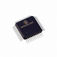
PIC16LC774/PQ Microchip Technology, PIC16LC774/PQ Datasheet - Page 117

PIC16LC774/PQ
Manufacturer Part Number
PIC16LC774/PQ
Description
IC MCU OTP 4KX14 A/D PWM 44-MQFP
Manufacturer
Microchip Technology
Series
PIC® 16Cr
Specifications of PIC16LC774/PQ
Core Processor
PIC
Core Size
8-Bit
Speed
20MHz
Connectivity
I²C, SPI, UART/USART
Peripherals
Brown-out Detect/Reset, POR, PWM, WDT
Number Of I /o
33
Program Memory Size
7KB (4K x 14)
Program Memory Type
OTP
Ram Size
256 x 8
Voltage - Supply (vcc/vdd)
2.5 V ~ 5.5 V
Data Converters
A/D 10x12b
Oscillator Type
External
Operating Temperature
0°C ~ 70°C
Package / Case
44-MQFP, 44-PQFP
Processor Series
PIC16LC
Core
PIC
Data Bus Width
8 bit
Data Ram Size
256 B
Interface Type
I2C, SPI, SSP, UART
Maximum Clock Frequency
20 MHz
Number Of Programmable I/os
33
Number Of Timers
3 bit
Operating Supply Voltage
2.5 V to 5.5 V
Maximum Operating Temperature
+ 70 C
Mounting Style
SMD/SMT
3rd Party Development Tools
52715-96, 52716-328, 52717-734
Development Tools By Supplier
ICE2000, DM163022
Minimum Operating Temperature
0 C
On-chip Adc
10 bit
Lead Free Status / RoHS Status
Lead free / RoHS Compliant
Eeprom Size
-
Lead Free Status / Rohs Status
Details
Available stocks
Company
Part Number
Manufacturer
Quantity
Price
Company:
Part Number:
PIC16LC774/PQ
Manufacturer:
Microchip Technology
Quantity:
10 000
11.0
The analog-to-digital (A/D) converter module has six
inputs for the PIC16C773 and ten for the PIC16C774.
The analog-to-digital converter (A/D) allows conver-
sion of an analog input signal to a corresponding
12-bit digital number. The A/D module has up to 10
analog inputs, which are multiplexed into one sample
and hold. The output of the sample and hold is the
input into the converter, which generates the result via
successive approximation. The analog reference volt-
ages are software selectable to either the device’s
analog
(AV
V
(VRH, VRL).
The A/D converter has a unique feature of being able to
operate while the device is in SLEEP mode. To operate
in sleep, the A/D conversion clock must be derived from
the A/D’s internal RC oscillator.
FIGURE 11-1: ADCON0 REGISTER (ADDRESS 1Fh).
REF
1999 Microchip Technology Inc.
DD
ADCS1
bit7
bit 7:6
bit 5:3,1 CHS3:CHS0: Analog Channel Select bits
bit 2:
bit 0:
- pins, or internal voltage references if available
R/W-0
/AV
ANALOG-TO-DIGITAL
CONVERTER (A/D) MODULE
positive
SS
), the voltage level on the V
ADCS1:ADCS0: A/D Conversion Clock Select bits
00 = Fosc/2
01 = Fosc/8
10 = Fosc/32
11 = F
0000 = channel 00 (AN0)
0001 = channel 01 (AN1)
0010 = channel 02 (AN2)
0011 = channel 03 (AN3)
0100 = channel 04 (AN4) (Reserved on 28-pin devices, do not use)
0101 = channel 05 (AN5) (Reserved on 28-pin devices, do not use)
0110 = channel 06 (AN6) (Reserved on 28-pin devices, do not use)
0111 = channel 07 (AN7) (Reserved on 28-pin devices, do not use)
1000 = channel 08 (AN8)
1001 = channel 09 (AN9)
1010, 1011, 1100, 1101, 1110,1111 are reserved, do not select.
GO/DONE: A/D Conversion Status bit
1 = A/D conversion cycle in progress. Setting this bit starts an A/D conversion cycle.
This bit is automatically cleared by hardware when the A/D conversion has completed.
0 = A/D conversion completed/not in progress
ADON: A/D On bit
1 = A/D converter module is operating
0 = A/D converter is shutoff and consumes no operating current
ADCS0
R/W-0
and
RC
(clock derived from an RC oscillator = 1 MHz max)
R/W-0
CHS2
negative
R/W-0
CHS1
supply
R/W-0
CHS0
REF
Advance Information
voltages
+
and
GO/DONE
R/W-0
The A/D module has four registers. These registers
are:
A device reset forces all registers to their reset state.
This forces the A/D module to be turned off and any
conversion is aborted.
11.1
The ADCON0 register, shown in
the operation of the A/D module. The ADCON1 regis-
ter, shown in
the port pins, the voltage reference configuration and
the result format. The port pins can be configured as
analog inputs or as digital I/O.
The combination of the ADRESH and ADRESL regis-
ters contain the result of the A/D conversion. The reg-
ister pair is referred to as the ADRES register. When
the A/D conversion is complete, the result is loaded
into
cleared, and the A/D interrupt flag ADIF is set. The
block diagram of the A/D module is shown in
Figure
R/W-0
CHS3
• A/D Result Register Low ADRESL
• A/D Result Register High ADRESH
• A/D Control Register 0 (ADCON0)
• A/D Control Register 1 (ADCON1)
ADRES, the GO/DONE bit
11-3.
Control Registers
bit 0
R/W-0
ADON
Figure
R =
11-2, configures the functions of
W =
- n =
PIC16C77X
Readable bit
Writable bit
Value at POR reset
Figure
DS30275A-page 117
(ADCON0<2>) is
11-1, controls


