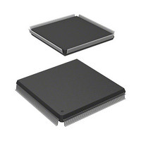
HD6417727F160V Renesas Electronics America, HD6417727F160V Datasheet - Page 41

HD6417727F160V
Manufacturer Part Number
HD6417727F160V
Description
MPU 3V 16K PB-FREE 240-QFP
Manufacturer
Renesas Electronics America
Series
SuperH® SH7700r
Datasheet
1.HD6417727BP100CV.pdf
(1098 pages)
Specifications of HD6417727F160V
Core Processor
SH-3 DSP
Core Size
32-Bit
Speed
160MHz
Connectivity
FIFO, SCI, SIO, SmartCard, USB
Peripherals
DMA, LCD, POR, WDT
Number Of I /o
104
Program Memory Type
ROMless
Ram Size
32K x 8
Voltage - Supply (vcc/vdd)
1.7 V ~ 2.05 V
Data Converters
A/D 6x10b; D/A 2x8b
Oscillator Type
Internal
Operating Temperature
-20°C ~ 75°C
Package / Case
240-QFP
Lead Free Status / RoHS Status
Lead free / RoHS Compliant
Eeprom Size
-
Program Memory Size
-
Available stocks
Company
Part Number
Manufacturer
Quantity
Price
Company:
Part Number:
HD6417727F160V
Manufacturer:
HITACHI
Quantity:
9
Company:
Part Number:
HD6417727F160V
Manufacturer:
Renesas Electronics America
Quantity:
10 000
Part Number:
HD6417727F160V
Manufacturer:
RENESAS/瑞萨
Quantity:
20 000
- Current page: 41 of 1098
- Download datasheet (7Mb)
Figure 9.11 Hardware Standby Mode Timing (CA = Low during WDT Operation
Section 10 On-Chip Oscillation Circuits
Figure 10.1 Block Diagram of Clock Pulse Generator .............................................................. 259
Figure 10.2 Block Diagram of the WDT ................................................................................... 271
Figure 10.3 Writing to WTCNT and WTCSR........................................................................... 275
Figure 10.4 Points for Attention when Using Crystal Resonator............................................... 277
Figure 10.5 Points for Attention when Using PLL Oscillator Circuit ....................................... 278
Section 11 Extend Clock Pulse Generator for USB (EXCPG)
Figure 11.1 Block Diagram of EXCPG ..................................................................................... 279
Section 12 Bus State Controller (BSC)
Figure 12.1 Corresponding to Logical Address Space and Physical Address Space................. 285
Figure 12.2 Corresponding to Logical Address Space and Physical Address Space................. 289
Figure 12.3 Physical Space Allocation ...................................................................................... 291
Figure 12.4 Writing to RFCR, RTCSR, RTCNT, and RTCOR................................................. 315
Figure 12.5 Basic Timing of Basic Interface ............................................................................. 326
Figure 12.6 Example of 32-Bit Data-Width Static RAM Connection ....................................... 327
Figure 12.7 Example of 16-Bit Data-Width Static RAM Connection ....................................... 328
Figure 12.8 Example of 8-Bit Data-Width Static RAM Connection ......................................... 328
Figure 12.9 Basic Interface Wait Timing (Software Wait Only)............................................... 329
Figure 12.10 Basic Interface Wait State Timing (Wait State Insertion by WAIT Signal
Figure 12.11 Example of 64-Mbit Synchronous DRAM Connection (32-Bit Bus Width) ......... 332
Figure 12.12 Example of 64-Mbit Synchronous DRAM (16-Bit Bus Width)............................. 333
Figure 12.13 Basic Timing for Synchronous DRAM Burst Read ............................................... 336
Figure 12.14 Synchronous DRAM Burst Read Wait Specification Timing ................................ 337
Figure 12.15 Basic Timing for Synchronous DRAM Single Read.............................................. 338
Figure 12.16 Basic Timing for Synchronous DRAM Burst Write .............................................. 339
Figure 12.17 Basic Timing for Synchronous DRAM Single Write............................................. 341
Figure 12.18 Auto-Refresh Operation ......................................................................................... 342
Figure 12.19 Synchronous DRAM Auto-Refresh Timing........................................................... 343
Figure 12.20 Synchronous DRAM Self-Refresh Timing ............................................................ 344
Figure 12.21 Synchronous DRAM Mode Write Timing ............................................................. 346
Figure 12.22 Burst ROM Wait Access Timing ........................................................................... 348
Figure 12.23 Burst ROM Basic Access Timing .......................................................................... 349
Figure 12.24 Example of PCMCIA Interface (If Internal PC Card Controller is not used.)........ 351
Figure 12.25 Basic Timing for PCMCIA Memory Card Interface.............................................. 353
Figure 12.26 Wait Timing for PCMCIA Memory Card Interface ............................................... 354
while Standby Mode is Cleared) ............................................................................ 256
WAITSEL = 1)....................................................................................................... 330
Rev.6.00 Mar. 27, 2009 Page xxxix of lvi
REJ09B0254-0600
Related parts for HD6417727F160V
Image
Part Number
Description
Manufacturer
Datasheet
Request
R

Part Number:
Description:
KIT STARTER FOR M16C/29
Manufacturer:
Renesas Electronics America
Datasheet:

Part Number:
Description:
KIT STARTER FOR R8C/2D
Manufacturer:
Renesas Electronics America
Datasheet:

Part Number:
Description:
R0K33062P STARTER KIT
Manufacturer:
Renesas Electronics America
Datasheet:

Part Number:
Description:
KIT STARTER FOR R8C/23 E8A
Manufacturer:
Renesas Electronics America
Datasheet:

Part Number:
Description:
KIT STARTER FOR R8C/25
Manufacturer:
Renesas Electronics America
Datasheet:

Part Number:
Description:
KIT STARTER H8S2456 SHARPE DSPLY
Manufacturer:
Renesas Electronics America
Datasheet:

Part Number:
Description:
KIT STARTER FOR R8C38C
Manufacturer:
Renesas Electronics America
Datasheet:

Part Number:
Description:
KIT STARTER FOR R8C35C
Manufacturer:
Renesas Electronics America
Datasheet:

Part Number:
Description:
KIT STARTER FOR R8CL3AC+LCD APPS
Manufacturer:
Renesas Electronics America
Datasheet:

Part Number:
Description:
KIT STARTER FOR RX610
Manufacturer:
Renesas Electronics America
Datasheet:

Part Number:
Description:
KIT STARTER FOR R32C/118
Manufacturer:
Renesas Electronics America
Datasheet:

Part Number:
Description:
KIT DEV RSK-R8C/26-29
Manufacturer:
Renesas Electronics America
Datasheet:

Part Number:
Description:
KIT STARTER FOR SH7124
Manufacturer:
Renesas Electronics America
Datasheet:

Part Number:
Description:
KIT STARTER FOR H8SX/1622
Manufacturer:
Renesas Electronics America
Datasheet:

Part Number:
Description:
KIT DEV FOR SH7203
Manufacturer:
Renesas Electronics America
Datasheet:


