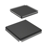
HD6417727F160V Renesas Electronics America, HD6417727F160V Datasheet - Page 215

HD6417727F160V
Manufacturer Part Number
HD6417727F160V
Description
MPU 3V 16K PB-FREE 240-QFP
Manufacturer
Renesas Electronics America
Series
SuperH® SH7700r
Datasheet
1.HD6417727BP100CV.pdf
(1098 pages)
Specifications of HD6417727F160V
Core Processor
SH-3 DSP
Core Size
32-Bit
Speed
160MHz
Connectivity
FIFO, SCI, SIO, SmartCard, USB
Peripherals
DMA, LCD, POR, WDT
Number Of I /o
104
Program Memory Type
ROMless
Ram Size
32K x 8
Voltage - Supply (vcc/vdd)
1.7 V ~ 2.05 V
Data Converters
A/D 6x10b; D/A 2x8b
Oscillator Type
Internal
Operating Temperature
-20°C ~ 75°C
Package / Case
240-QFP
Lead Free Status / RoHS Status
Lead free / RoHS Compliant
Eeprom Size
-
Program Memory Size
-
Available stocks
Company
Part Number
Manufacturer
Quantity
Price
Company:
Part Number:
HD6417727F160V
Manufacturer:
HITACHI
Quantity:
9
Company:
Part Number:
HD6417727F160V
Manufacturer:
Renesas Electronics America
Quantity:
10 000
Part Number:
HD6417727F160V
Manufacturer:
RENESAS/瑞萨
Quantity:
20 000
- Current page: 215 of 1098
- Download datasheet (7Mb)
5.3.5
When the U bit of the entry to be replaced in the write-back mode is 1, it must be written back to
the external memory. To increase performance, the entry to be replaced is first transferred to the
write-back buffer and fetching of new entries to the cache takes priority over writing back to the
external memory. During the write back cycles, the cache can be accessed. The write-back buffer
can hold one line of the cache data (16 bytes) and its physical address. Figure 5.5 shows the
configuration of the write-back buffer.
5.3.6
Use software to ensure coherency between the cache and the external memory. When memory
shared by this LSI and another device is accessed, the latest data may be in a write-back mode
cache, so invalidate the entry that includes the latest data in the cache, generate a write back, and
update the data in memory before using it. When the caching area is updated by a device other
than the SH7727, invalidate the entry that includes the updated data in the cache.
5.4
To allow software management of the cache, cache contents can be read and written by means of
MOV instructions in the privileged mode. The cache is mapped onto the P4 area in logical address
space. The address array is mapped onto addresses H'F0000000 to H'F0FFFFFF, and the data
array onto addresses H'F1000000 to H'F1FFFFFF. Only longword can be used as the access size
for the address array and data array, and instruction fetches cannot be performed.
5.4.1
The address array is mapped onto H'F0000000 to H'F0FFFFFF. To access an address array, the
32-bit address field (for read/write accesses) and 32-bit data field (for write accesses) must be
specified. The address field specifies information for selecting the entry to be accessed; the data
field specifies the address, V bit, U bit, and LRU bits to be written to the address array ((1) in
figure 5.6).
Write-Back Buffer
Coherency of Cache and External Memory
Memory-Mapped Cache
Address Array
PA (31 to 4):
Longword 0 to 3:
PA (31 to 4)
Figure 5.5 Write-Back Buffer Configuration
Longword 0
Physical address written to external memory
The line of cache data to be written to
external memory
Longword 1
Rev.6.00 Mar. 27, 2009 Page 157 of 1036
Longword 2
Longword 3
REJ09B0254-0600
Section 5 Cache
Related parts for HD6417727F160V
Image
Part Number
Description
Manufacturer
Datasheet
Request
R

Part Number:
Description:
KIT STARTER FOR M16C/29
Manufacturer:
Renesas Electronics America
Datasheet:

Part Number:
Description:
KIT STARTER FOR R8C/2D
Manufacturer:
Renesas Electronics America
Datasheet:

Part Number:
Description:
R0K33062P STARTER KIT
Manufacturer:
Renesas Electronics America
Datasheet:

Part Number:
Description:
KIT STARTER FOR R8C/23 E8A
Manufacturer:
Renesas Electronics America
Datasheet:

Part Number:
Description:
KIT STARTER FOR R8C/25
Manufacturer:
Renesas Electronics America
Datasheet:

Part Number:
Description:
KIT STARTER H8S2456 SHARPE DSPLY
Manufacturer:
Renesas Electronics America
Datasheet:

Part Number:
Description:
KIT STARTER FOR R8C38C
Manufacturer:
Renesas Electronics America
Datasheet:

Part Number:
Description:
KIT STARTER FOR R8C35C
Manufacturer:
Renesas Electronics America
Datasheet:

Part Number:
Description:
KIT STARTER FOR R8CL3AC+LCD APPS
Manufacturer:
Renesas Electronics America
Datasheet:

Part Number:
Description:
KIT STARTER FOR RX610
Manufacturer:
Renesas Electronics America
Datasheet:

Part Number:
Description:
KIT STARTER FOR R32C/118
Manufacturer:
Renesas Electronics America
Datasheet:

Part Number:
Description:
KIT DEV RSK-R8C/26-29
Manufacturer:
Renesas Electronics America
Datasheet:

Part Number:
Description:
KIT STARTER FOR SH7124
Manufacturer:
Renesas Electronics America
Datasheet:

Part Number:
Description:
KIT STARTER FOR H8SX/1622
Manufacturer:
Renesas Electronics America
Datasheet:

Part Number:
Description:
KIT DEV FOR SH7203
Manufacturer:
Renesas Electronics America
Datasheet:


