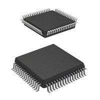
DF36034HJV Renesas Electronics America, DF36034HJV Datasheet - Page 261

DF36034HJV
Manufacturer Part Number
DF36034HJV
Description
MCU 3/5V 32K J-TEMP PB-FREE 64-Q
Manufacturer
Renesas Electronics America
Series
H8® H8/300H Tinyr
Specifications of DF36034HJV
Core Processor
H8/300H
Core Size
16-Bit
Speed
20MHz
Connectivity
CAN, SCI, SSU
Peripherals
PWM, WDT
Number Of I /o
45
Program Memory Size
32KB (32K x 8)
Program Memory Type
FLASH
Ram Size
2K x 8
Voltage - Supply (vcc/vdd)
3 V ~ 5.5 V
Data Converters
A/D 8x10b
Oscillator Type
Internal
Operating Temperature
-40°C ~ 85°C
Package / Case
64-QFP
For Use With
R0K436079S000BE - KIT DEV FOR H8/36079 W/COMPILER
Lead Free Status / RoHS Status
Lead free / RoHS Compliant
Eeprom Size
-
- Current page: 261 of 594
- Download datasheet (4Mb)
Figures 12.42 and 12.43 show the operation examples when buffer operation has been designated
for GRB_0 and GRD_0 in complementary PWM mode. These are examples when a PWM
waveform of 0% duty is created by using the buffer operation and performing GRD_0 GRA_0.
Data is transferred from GRD_0 to GRB_0 according to the settings of CMD_0 and CMD_1 when
TCNT_0 and GRA_0 are compared and their contents match or when TCNT_1 underflows.
However, when GRD_0 GRA_0, data is transferred from GRD_0 to GRB_0 when TCNT_1
underflows regardless of the setting of CMD_0 and CMD_1. When GRD_0 = H'0000, data is
transferred from GRD_0 to GRB_0 when TCNT_0 and GRA_0 are compared and their contents
match regardless of the settings of CMD_0 and CMD_1.
GRA_0
H'0999
H'0000
FTIOB0
FTIOD0
GRD_0
GRB_0
TCNT values
(Buffer Operation in Complementary PWM Mode CMD1 = CMD0 = 1)
H'0999
H'0999
TCNT_0
TCNT_1
H'0999
Figure 12.42 Buffer Operation (3)
H'1FFF
H'1FFF
H'0999
GRB_0 (When restored, data will be transferred
Rev. 4.00 Mar. 15, 2006 Page 227 of 556
H'0999
to the saved location regardless of the
CMD1 and CMD0 values)
Time
Section 12 Timer Z
REJ09B0026-0400
Related parts for DF36034HJV
Image
Part Number
Description
Manufacturer
Datasheet
Request
R

Part Number:
Description:
Headers & Wire Housings 20P PLUG METAL COVER
Manufacturer:
Hirose Electric Co Ltd

Part Number:
Description:
Headers & Wire Housings 25P PLUG METAL COVER
Manufacturer:
Hirose Electric Co Ltd

Part Number:
Description:
Headers & Wire Housings 15P PLUG METAL COVER
Manufacturer:
Hirose Electric Co Ltd

Part Number:
Description:
0.4 Mm Pitch, 1.5 Mm Mated Height, Board-to-fine Coaxial Cable Connectors
Manufacturer:
Hirose Electric
Datasheet:

Part Number:
Description:
CONN RECEPT 40POS 0.4MM SMD GOLD
Manufacturer:
Hirose Electric Co Ltd
Datasheet:

Part Number:
Description:
KIT STARTER FOR M16C/29
Manufacturer:
Renesas Electronics America
Datasheet:

Part Number:
Description:
KIT STARTER FOR R8C/2D
Manufacturer:
Renesas Electronics America
Datasheet:

Part Number:
Description:
R0K33062P STARTER KIT
Manufacturer:
Renesas Electronics America
Datasheet:

Part Number:
Description:
KIT STARTER FOR R8C/23 E8A
Manufacturer:
Renesas Electronics America
Datasheet:

Part Number:
Description:
KIT STARTER FOR R8C/25
Manufacturer:
Renesas Electronics America
Datasheet:

Part Number:
Description:
KIT STARTER H8S2456 SHARPE DSPLY
Manufacturer:
Renesas Electronics America
Datasheet:

Part Number:
Description:
KIT STARTER FOR R8C38C
Manufacturer:
Renesas Electronics America
Datasheet:

Part Number:
Description:
KIT STARTER FOR R8C35C
Manufacturer:
Renesas Electronics America
Datasheet:

Part Number:
Description:
KIT STARTER FOR R8CL3AC+LCD APPS
Manufacturer:
Renesas Electronics America
Datasheet:

Part Number:
Description:
KIT STARTER FOR RX610
Manufacturer:
Renesas Electronics America
Datasheet:


