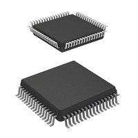
DF36034HJV Renesas Electronics America, DF36034HJV Datasheet - Page 244

DF36034HJV
Manufacturer Part Number
DF36034HJV
Description
MCU 3/5V 32K J-TEMP PB-FREE 64-Q
Manufacturer
Renesas Electronics America
Series
H8® H8/300H Tinyr
Specifications of DF36034HJV
Core Processor
H8/300H
Core Size
16-Bit
Speed
20MHz
Connectivity
CAN, SCI, SSU
Peripherals
PWM, WDT
Number Of I /o
45
Program Memory Size
32KB (32K x 8)
Program Memory Type
FLASH
Ram Size
2K x 8
Voltage - Supply (vcc/vdd)
3 V ~ 5.5 V
Data Converters
A/D 8x10b
Oscillator Type
Internal
Operating Temperature
-40°C ~ 85°C
Package / Case
64-QFP
For Use With
R0K436079S000BE - KIT DEV FOR H8/36079 W/COMPILER
Lead Free Status / RoHS Status
Lead free / RoHS Compliant
Eeprom Size
-
- Current page: 244 of 594
- Download datasheet (4Mb)
Section 12 Timer Z
12.4.7
Three PWM waveforms for non-overlapped normal and counter phases are output by combining
channels 0 and 1.
In complementary PWM mode, the FTIOB0 to FTIOD0 and FTIOA1 to FTIOD1 pins become
PWM-output pins automatically. TCNT_0 and TCNT_1 perform an increment or decrement
operation. Tables 12.6 and 12.7 show the output pins and register settings in complementary PWM
mode, respectively.
Figure 12.29 shows the example of complementary PWM mode setting procedure.
Table 12.6 Output Pins in Complementary PWM Mode
Rev. 4.00 Mar. 15, 2006 Page 210 of 556
REJ09B0026-0400
Channel
0
0
0
1
1
1
1
Complementary PWM Mode
Pin Name
FTIOC0
FTIOB0
FTIOD0
FTIOA1
FTIOC1
FTIOB1
FTIOD1
I/O
Output
Output
Output
Output
Output
Output
Output
Toggle output in synchronous with PWM cycle
PWM output 1
PWM output 1 (counter-phase waveform non-overlapped
PWM output 2
PWM output 2 (counter-phase waveform non-overlapped
PWM output 3
PWM output 3 (counter-phase waveform non-overlapped
Pin Function
with PWM output 1)
with PWM output 2)
with PWM output 3)
Related parts for DF36034HJV
Image
Part Number
Description
Manufacturer
Datasheet
Request
R

Part Number:
Description:
Headers & Wire Housings 20P PLUG METAL COVER
Manufacturer:
Hirose Electric Co Ltd

Part Number:
Description:
Headers & Wire Housings 25P PLUG METAL COVER
Manufacturer:
Hirose Electric Co Ltd

Part Number:
Description:
Headers & Wire Housings 15P PLUG METAL COVER
Manufacturer:
Hirose Electric Co Ltd

Part Number:
Description:
0.4 Mm Pitch, 1.5 Mm Mated Height, Board-to-fine Coaxial Cable Connectors
Manufacturer:
Hirose Electric
Datasheet:

Part Number:
Description:
CONN RECEPT 40POS 0.4MM SMD GOLD
Manufacturer:
Hirose Electric Co Ltd
Datasheet:

Part Number:
Description:
KIT STARTER FOR M16C/29
Manufacturer:
Renesas Electronics America
Datasheet:

Part Number:
Description:
KIT STARTER FOR R8C/2D
Manufacturer:
Renesas Electronics America
Datasheet:

Part Number:
Description:
R0K33062P STARTER KIT
Manufacturer:
Renesas Electronics America
Datasheet:

Part Number:
Description:
KIT STARTER FOR R8C/23 E8A
Manufacturer:
Renesas Electronics America
Datasheet:

Part Number:
Description:
KIT STARTER FOR R8C/25
Manufacturer:
Renesas Electronics America
Datasheet:

Part Number:
Description:
KIT STARTER H8S2456 SHARPE DSPLY
Manufacturer:
Renesas Electronics America
Datasheet:

Part Number:
Description:
KIT STARTER FOR R8C38C
Manufacturer:
Renesas Electronics America
Datasheet:

Part Number:
Description:
KIT STARTER FOR R8C35C
Manufacturer:
Renesas Electronics America
Datasheet:

Part Number:
Description:
KIT STARTER FOR R8CL3AC+LCD APPS
Manufacturer:
Renesas Electronics America
Datasheet:

Part Number:
Description:
KIT STARTER FOR RX610
Manufacturer:
Renesas Electronics America
Datasheet:


