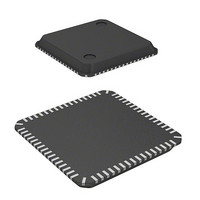
DF2210CUNP24V Renesas Electronics America, DF2210CUNP24V Datasheet - Page 583

DF2210CUNP24V
Manufacturer Part Number
DF2210CUNP24V
Description
MCU 16BIT FLASH 3V 32K 64-QFN
Manufacturer
Renesas Electronics America
Series
H8® H8S/2200r
Datasheet
1.DF2218UTF24V.pdf
(758 pages)
Specifications of DF2210CUNP24V
Core Processor
H8S/2000
Core Size
16-Bit
Speed
24MHz
Connectivity
SCI, SmartCard, USB
Peripherals
DMA, POR, PWM, WDT
Number Of I /o
37
Program Memory Size
32KB (32K x 8)
Program Memory Type
FLASH
Ram Size
4K x 8
Voltage - Supply (vcc/vdd)
2.7 V ~ 3.6 V
Data Converters
A/D 6x10b
Oscillator Type
External
Operating Temperature
-20°C ~ 75°C
Package / Case
64-QFN
Lead Free Status / RoHS Status
Lead free / RoHS Compliant
Eeprom Size
-
Available stocks
Company
Part Number
Manufacturer
Quantity
Price
Company:
Part Number:
DF2210CUNP24V
Manufacturer:
Renesas Electronics America
Quantity:
135
- Current page: 583 of 758
- Download datasheet (5Mb)
14.8
14.8.1
1. If UEDR0o and UEDR2 are displayed using the I/O register window function, or the like, the
2. In the E6000, since the USB module is mounted on the external extended board and accessed
• USB operation is not supported in the H8S/2218 Group’s mode 7 (single-chip mode).
• When using the USB module in the H8S/2218 Group’s mode 6 (on-chip ROM-enabled mode)
• When using the USB module in the H8S/2218 Group’s modes 4 and 5 (on-chip ROM-disabled
14.8.2
The USB module’s interface is based on the bus specifications of external area 6. Accordingly,
before accessing the USB module, area 6 must be specified as having an 8-bit bus width and 3-
state access using the bus controller register.
Address H'C00100 to H'DFFFFF is for USB reserved area and thus access prohibited.
14.8.3
The main clock of this LSI must be 24 MHz or 16 MHz. This 24-MHz main clock, used as base
clock, is doubled in the on-chip PLL circuit or this 16-MHz main clock, also used as base clock, is
tripled in the on-chip PLL circuit, to generate the 48-MHz USB operating clock. Since the USB
module does not support medium-speed mode, sleep mode, watch mode, subactive mode, and
subsleep mode, make sure to use full-speed mode.
EP0o FIFO or EP2 FIFO read pointer will not operate properly, preventing UEDR0o, UESZ0o,
UEDR2, and UESZ2 from being read correctly. Therefore, UEDR0o and UEDR2 should not
be displayed.
as an external module, there are some limitations as shown below. These limitations do not
apply to the E10A or to product chips.
or the H8S/2212 Group’s mode 7 (single-chip mode), CS6 and A9 to A0 are input pins in the
initial status. Therefore, CS6 and A9 to A0 must be set as output pins (= B'0010) by setting
P72DDR to 1, AE3 to AE0 to B'0010, and PC7DDR to PC0DDR to H'FF before accessing the
USB module.
mode), CS6 and A9 to A8 must be set as output pins by setting P72DDR to 1 and AE3 to AE0
to B'0010.
Usage Notes
Emulator Usage Notes
Bus Interface
Operating Frequency
Rev.7.00 Dec. 24, 2008 Page 527 of 698
REJ09B0074-0700
Related parts for DF2210CUNP24V
Image
Part Number
Description
Manufacturer
Datasheet
Request
R

Part Number:
Description:
KIT STARTER FOR M16C/29
Manufacturer:
Renesas Electronics America
Datasheet:

Part Number:
Description:
KIT STARTER FOR R8C/2D
Manufacturer:
Renesas Electronics America
Datasheet:

Part Number:
Description:
R0K33062P STARTER KIT
Manufacturer:
Renesas Electronics America
Datasheet:

Part Number:
Description:
KIT STARTER FOR R8C/23 E8A
Manufacturer:
Renesas Electronics America
Datasheet:

Part Number:
Description:
KIT STARTER FOR R8C/25
Manufacturer:
Renesas Electronics America
Datasheet:

Part Number:
Description:
KIT STARTER H8S2456 SHARPE DSPLY
Manufacturer:
Renesas Electronics America
Datasheet:

Part Number:
Description:
KIT STARTER FOR R8C38C
Manufacturer:
Renesas Electronics America
Datasheet:

Part Number:
Description:
KIT STARTER FOR R8C35C
Manufacturer:
Renesas Electronics America
Datasheet:

Part Number:
Description:
KIT STARTER FOR R8CL3AC+LCD APPS
Manufacturer:
Renesas Electronics America
Datasheet:

Part Number:
Description:
KIT STARTER FOR RX610
Manufacturer:
Renesas Electronics America
Datasheet:

Part Number:
Description:
KIT STARTER FOR R32C/118
Manufacturer:
Renesas Electronics America
Datasheet:

Part Number:
Description:
KIT DEV RSK-R8C/26-29
Manufacturer:
Renesas Electronics America
Datasheet:

Part Number:
Description:
KIT STARTER FOR SH7124
Manufacturer:
Renesas Electronics America
Datasheet:

Part Number:
Description:
KIT STARTER FOR H8SX/1622
Manufacturer:
Renesas Electronics America
Datasheet:

Part Number:
Description:
KIT DEV FOR SH7203
Manufacturer:
Renesas Electronics America
Datasheet:


