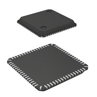
DF2210CUNP24V Renesas Electronics America, DF2210CUNP24V Datasheet - Page 130

DF2210CUNP24V
Manufacturer Part Number
DF2210CUNP24V
Description
MCU 16BIT FLASH 3V 32K 64-QFN
Manufacturer
Renesas Electronics America
Series
H8® H8S/2200r
Datasheet
1.DF2218UTF24V.pdf
(758 pages)
Specifications of DF2210CUNP24V
Core Processor
H8S/2000
Core Size
16-Bit
Speed
24MHz
Connectivity
SCI, SmartCard, USB
Peripherals
DMA, POR, PWM, WDT
Number Of I /o
37
Program Memory Size
32KB (32K x 8)
Program Memory Type
FLASH
Ram Size
4K x 8
Voltage - Supply (vcc/vdd)
2.7 V ~ 3.6 V
Data Converters
A/D 6x10b
Oscillator Type
External
Operating Temperature
-20°C ~ 75°C
Package / Case
64-QFN
Lead Free Status / RoHS Status
Lead free / RoHS Compliant
Eeprom Size
-
Available stocks
Company
Part Number
Manufacturer
Quantity
Price
Company:
Part Number:
DF2210CUNP24V
Manufacturer:
Renesas Electronics America
Quantity:
135
- Current page: 130 of 758
- Download datasheet (5Mb)
3.3
3.3.1
The CPU can access a 16-Mbyte address space in advanced mode. The on-chip ROM is disabled.
Pins P13 to P10, and ports A, B, and C function as an address bus, ports D and E function as a data
bus, and part of port F carries bus control signals.
Pins P13 to P11 function as input ports immediately after a reset. Pin 10 and ports A and B
function as address (A20 to A8) outputs immediately after a reset. Address (A23 to A21) output
can be enabled or disabled by bits AE3 to AE0 in the pin function control register (PFCR)
regardless of the corresponding data direction register (DDR) values. Pins for which address
output is disabled among pins P13 to P10 and in ports A and B become port outputs when the
corresponding DDR bits are set to 1.
Port C always has an address (A7 to A0) output function.
The initial bus mode after a reset is 16 bits, with 16-bit access to all areas. However, note that if 8-
bit access is designated by the bus controller for all areas, the bus mode switches to 8 bits.
3.3.2
The CPU can access a 16-Mbyte address space in advanced mode. The on-chip ROM is disabled.
Pins P13 to P10, and ports A, B, and C function as an address bus, ports D and E function as a data
bus, and part of port F carries bus control signals.
Pins P13 to P11 function as input ports immediately after a reset. Pin 10 and ports A and B
function as address (A20 to A8) outputs immediately after a reset. Address (A23 to A21) output
can be enabled or disabled by bits AE3 to AE0 in the pin function control register (PFCR)
regardless of the corresponding data direction register (DDR) values. Pins for which address
output is disabled among pins P13 to P10 and in ports A and B become port outputs when the
corresponding DDR bits are set to 1.
Port C always has an address (A7 to A0) output function.
The initial bus mode after a reset is 8 bits, with 8-bit access to all areas. However, note that if 16-
bit access is designated by the bus controller for any area, the bus mode switches to 16 bits and
port E becomes a data bus.
Rev.7.00 Dec. 24, 2008 Page 74 of 698
REJ09B0074-0700
Mode 4 (Supported Only by the H8S/2218 Group)
Mode 5 (Supported Only by the H8S/2218 Group)
Operating Mode Descriptions
Related parts for DF2210CUNP24V
Image
Part Number
Description
Manufacturer
Datasheet
Request
R

Part Number:
Description:
KIT STARTER FOR M16C/29
Manufacturer:
Renesas Electronics America
Datasheet:

Part Number:
Description:
KIT STARTER FOR R8C/2D
Manufacturer:
Renesas Electronics America
Datasheet:

Part Number:
Description:
R0K33062P STARTER KIT
Manufacturer:
Renesas Electronics America
Datasheet:

Part Number:
Description:
KIT STARTER FOR R8C/23 E8A
Manufacturer:
Renesas Electronics America
Datasheet:

Part Number:
Description:
KIT STARTER FOR R8C/25
Manufacturer:
Renesas Electronics America
Datasheet:

Part Number:
Description:
KIT STARTER H8S2456 SHARPE DSPLY
Manufacturer:
Renesas Electronics America
Datasheet:

Part Number:
Description:
KIT STARTER FOR R8C38C
Manufacturer:
Renesas Electronics America
Datasheet:

Part Number:
Description:
KIT STARTER FOR R8C35C
Manufacturer:
Renesas Electronics America
Datasheet:

Part Number:
Description:
KIT STARTER FOR R8CL3AC+LCD APPS
Manufacturer:
Renesas Electronics America
Datasheet:

Part Number:
Description:
KIT STARTER FOR RX610
Manufacturer:
Renesas Electronics America
Datasheet:

Part Number:
Description:
KIT STARTER FOR R32C/118
Manufacturer:
Renesas Electronics America
Datasheet:

Part Number:
Description:
KIT DEV RSK-R8C/26-29
Manufacturer:
Renesas Electronics America
Datasheet:

Part Number:
Description:
KIT STARTER FOR SH7124
Manufacturer:
Renesas Electronics America
Datasheet:

Part Number:
Description:
KIT STARTER FOR H8SX/1622
Manufacturer:
Renesas Electronics America
Datasheet:

Part Number:
Description:
KIT DEV FOR SH7203
Manufacturer:
Renesas Electronics America
Datasheet:


