HD64F3672FPIV Renesas Electronics America, HD64F3672FPIV Datasheet - Page 12
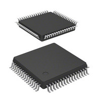
HD64F3672FPIV
Manufacturer Part Number
HD64F3672FPIV
Description
MCU 3/5V 16K I-TEMP PB-FREE 64-L
Manufacturer
Renesas Electronics America
Series
H8® H8/300H Tinyr
Datasheet
1.HD64F3672FXV.pdf
(334 pages)
Specifications of HD64F3672FPIV
Core Processor
H8/300H
Core Size
16-Bit
Speed
16MHz
Connectivity
SCI
Peripherals
PWM, WDT
Number Of I /o
26
Program Memory Size
16KB (16K x 8)
Program Memory Type
FLASH
Ram Size
2K x 8
Voltage - Supply (vcc/vdd)
3 V ~ 5.5 V
Data Converters
A/D 4x10b
Oscillator Type
Internal
Operating Temperature
-40°C ~ 85°C
Package / Case
64-LQFP
For Use With
R0K436079S000BE - KIT DEV FOR H8/36079 W/COMPILER
Lead Free Status / RoHS Status
Lead free / RoHS Compliant
Eeprom Size
-


3.3
3.4
3.5
Section 4 Address Break ..................................................................................... 55
4.1
4.2
4.3
Section 5 Clock Pulse Generators ....................................................................... 65
5.1
5.2
5.3
Section 6 Power-Down Modes............................................................................ 69
6.1
6.2
Rev.4.00 Nov. 02, 2005 Page x of xxiv
3.2.5
Reset Exception Handling.................................................................................................... 48
Interrupt Exception Handling .............................................................................................. 48
3.4.1
3.4.2
3.4.3
3.4.4
Usage Notes ......................................................................................................................... 53
3.5.1
3.5.2
3.5.3
Register Descriptions........................................................................................................... 55
4.1.1
4.1.2
4.1.3
4.1.4
Operation ............................................................................................................................. 59
Usage Notes ......................................................................................................................... 61
System Clock Generator ...................................................................................................... 65
5.1.1
5.1.2
5.1.3
Prescalers ............................................................................................................................. 67
5.2.1
Usage Notes ......................................................................................................................... 67
5.3.1
5.3.2
Register Descriptions........................................................................................................... 70
6.1.1
6.1.2
6.1.3
Mode Transitions and States of LSI..................................................................................... 74
6.2.1
6.2.2
Wakeup Interrupt Flag Register (IWPR) ................................................................ 47
External Interrupts .................................................................................................. 48
Internal Interrupts ................................................................................................... 49
Interrupt Handling Sequence .................................................................................. 50
Interrupt Response Time......................................................................................... 51
Interrupts after Reset............................................................................................... 53
Notes on Stack Area Use ........................................................................................ 53
Notes on Rewriting Port Mode Registers ............................................................... 53
Address Break Control Register (ABRKCR) ......................................................... 56
Address Break Status Register (ABRKSR) ............................................................ 57
Break Address Registers (BARH, BARL).............................................................. 58
Break Data Registers (BDRH, BDRL) ................................................................... 58
Connecting Crystal Resonator ................................................................................ 66
Connecting Ceramic Resonator .............................................................................. 66
External Clock Input Method ................................................................................. 67
Prescaler S .............................................................................................................. 67
Note on Resonators................................................................................................. 67
Notes on Board Design ........................................................................................... 68
System Control Register 1 (SYSCR1) .................................................................... 70
System Control Register 2 (SYSCR2) .................................................................... 72
Module Standby Control Register 1 (MSTCR1) .................................................... 73
Sleep Mode ............................................................................................................. 76
Standby Mode......................................................................................................... 76
Related parts for HD64F3672FPIV
Image
Part Number
Description
Manufacturer
Datasheet
Request
R


Part Number:
Description:
KIT STARTER FOR M16C/29
Manufacturer:
Renesas Electronics America
Datasheet:

Part Number:
Description:
KIT STARTER FOR R8C/2D
Manufacturer:
Renesas Electronics America
Datasheet:

Part Number:
Description:
R0K33062P STARTER KIT
Manufacturer:
Renesas Electronics America
Datasheet:

Part Number:
Description:
KIT STARTER FOR R8C/23 E8A
Manufacturer:
Renesas Electronics America
Datasheet:

Part Number:
Description:
KIT STARTER FOR R8C/25
Manufacturer:
Renesas Electronics America
Datasheet:

Part Number:
Description:
KIT STARTER H8S2456 SHARPE DSPLY
Manufacturer:
Renesas Electronics America
Datasheet:

Part Number:
Description:
KIT STARTER FOR R8C38C
Manufacturer:
Renesas Electronics America
Datasheet:

Part Number:
Description:
KIT STARTER FOR R8C35C
Manufacturer:
Renesas Electronics America
Datasheet:

Part Number:
Description:
KIT STARTER FOR R8CL3AC+LCD APPS
Manufacturer:
Renesas Electronics America
Datasheet:
Part Number:
Description:
KIT STARTER FOR RX610
Manufacturer:
Renesas Electronics America
Datasheet:

Part Number:
Description:
KIT STARTER FOR R32C/118
Manufacturer:
Renesas Electronics America
Datasheet:

Part Number:
Description:
KIT DEV RSK-R8C/26-29
Manufacturer:
Renesas Electronics America
Datasheet:

Part Number:
Description:
KIT STARTER FOR SH7124
Manufacturer:
Renesas Electronics America
Datasheet:

Part Number:
Description:
KIT STARTER FOR H8SX/1622
Manufacturer:
Renesas Electronics America
Datasheet: