MCHC908JW32FAE Freescale Semiconductor, MCHC908JW32FAE Datasheet - Page 78
MCHC908JW32FAE
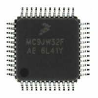
Manufacturer Part Number
MCHC908JW32FAE
Description
IC MCU 32K FLASH 8MHZ 48-LQFP
Manufacturer
Freescale Semiconductor
Series
HC08r
Datasheet
1.RD3152MMA7260Q.pdf
(232 pages)
Specifications of MCHC908JW32FAE
Core Processor
HC08
Core Size
8-Bit
Speed
8MHz
Connectivity
SPI, USB
Peripherals
LED, LVD, POR, PWM
Number Of I /o
29
Program Memory Size
32KB (32K x 8)
Program Memory Type
FLASH
Ram Size
1K x 8
Voltage - Supply (vcc/vdd)
3.5 V ~ 5.5 V
Oscillator Type
Internal
Operating Temperature
0°C ~ 70°C
Package / Case
48-LQFP
Controller Family/series
HC08
No. Of I/o's
48
Ram Memory Size
1KB
Cpu Speed
8MHz
No. Of Timers
1
Embedded Interface Type
SPI
Rohs Compliant
Yes
Processor Series
HC08JW
Core
HC08
Data Bus Width
8 bit
Data Ram Size
1 KB
Interface Type
SPI, USB
Number Of Programmable I/os
29
Number Of Timers
2
Maximum Operating Temperature
+ 70 C
Mounting Style
SMD/SMT
Development Tools By Supplier
FSICEBASE, DEMO908GZ60E, M68EML08GZE, KITUSBSPIDGLEVME, KITUSBSPIEVME, KIT33810EKEVME
Minimum Operating Temperature
0 C
Lead Free Status / RoHS Status
Lead free / RoHS Compliant
Eeprom Size
-
Data Converters
-
Lead Free Status / Rohs Status
Details
Available stocks
Company
Part Number
Manufacturer
Quantity
Price

Company:
Part Number:
MCHC908JW32FAE
Manufacturer:
Freescale Semiconductor
Quantity:
10 000
Part Number:
MCHC908JW32FAE
Manufacturer:
FREESCALE
Quantity:
20 000


System Integration Module (SIM)
6.2.2 Clock Start-up from POR or LVI Reset
When the power-on reset module or the low-voltage inhibit module generates a reset, the clocks to the
CPU and peripherals are inactive and held in an inactive phase until after the 4096 CGMXCLK cycle POR
timeout has completed. The RST pin is driven low by the SIM during this entire period. The IBUS clocks
start upon completion of the timeout.
6.2.3 Clocks in Stop Mode and Wait Mode
Upon exit from stop mode by an interrupt, break, or reset, the SIM allows CGMXCLK to clock the SIM
counter. The CPU and peripheral clocks do not become active until after the stop delay timeout. This
timeout is selectable as 4096 or 32 CGMXCLK cycles. (See
In wait mode, the CPU clocks are inactive. The SIM also produces two sets of clocks for other modules.
Refer to the wait mode subsection of each module to see if the module is active or inactive in wait mode.
Some modules can be programmed to be active in wait mode.
6.3 Reset and System Initialization
The MCU has these reset sources:
All of these resets produce the vector $FFFE:$FFFF ($FEFE:$FEFF in monitor mode) and assert the
internal reset signal (IRST). IRST causes all registers to be returned to their default values and all
modules to be returned to their reset states.
An internal reset clears the SIM counter (see
the resets sets a corresponding bit in the SIM reset status register (SRSR). (See
6.3.1 External Pin Reset
The RST pin circuit includes an internal pull-up device. Pulling the asynchronous RST pin low halts all
processing. The PIN bit of the SIM reset status register (SRSR) is set as long as RST is held low for at
least the minimum t
shows the relative timing.
78
•
•
•
•
•
•
•
Power-on reset module (POR)
External reset pin (RST)
Computer operating properly module (COP)
Low-voltage inhibit module (LVI)
Illegal opcode
Illegal address
Universal serial bus module (USB)
Reset Recovery Type
RL
All others
POR/LVI
time and no other reset sources are present. See
MC68HC908JW32 Data Sheet, Rev. 6
Table 6-2. Reset Recovery
6.4 SIM
Actual Number of Cycles
Counter), but an external reset does not. Each of
4163 (4096 + 64 + 3)
67 (64 + 3)
6.6.2 Stop
Mode.)
Table 6-2
6.7 SIM
for details.
Freescale Semiconductor
Registers.)
Figure 6-4
Related parts for MCHC908JW32FAE
Image
Part Number
Description
Manufacturer
Datasheet
Request
R

Part Number:
Description:
Manufacturer:
Freescale Semiconductor, Inc
Datasheet:
Part Number:
Description:
Manufacturer:
Freescale Semiconductor, Inc
Datasheet:
Part Number:
Description:
Manufacturer:
Freescale Semiconductor, Inc
Datasheet:
Part Number:
Description:
Manufacturer:
Freescale Semiconductor, Inc
Datasheet:
Part Number:
Description:
Manufacturer:
Freescale Semiconductor, Inc
Datasheet:
Part Number:
Description:
Manufacturer:
Freescale Semiconductor, Inc
Datasheet:
Part Number:
Description:
Manufacturer:
Freescale Semiconductor, Inc
Datasheet:
Part Number:
Description:
Manufacturer:
Freescale Semiconductor, Inc
Datasheet:
Part Number:
Description:
Manufacturer:
Freescale Semiconductor, Inc
Datasheet:
Part Number:
Description:
Manufacturer:
Freescale Semiconductor, Inc
Datasheet:
Part Number:
Description:
Manufacturer:
Freescale Semiconductor, Inc
Datasheet:
Part Number:
Description:
Manufacturer:
Freescale Semiconductor, Inc
Datasheet:
Part Number:
Description:
Manufacturer:
Freescale Semiconductor, Inc
Datasheet:
Part Number:
Description:
Manufacturer:
Freescale Semiconductor, Inc
Datasheet:
Part Number:
Description:
Manufacturer:
Freescale Semiconductor, Inc
Datasheet: