MCHC908JW32FAE Freescale Semiconductor, MCHC908JW32FAE Datasheet - Page 172
MCHC908JW32FAE
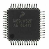
Manufacturer Part Number
MCHC908JW32FAE
Description
IC MCU 32K FLASH 8MHZ 48-LQFP
Manufacturer
Freescale Semiconductor
Series
HC08r
Datasheet
1.RD3152MMA7260Q.pdf
(232 pages)
Specifications of MCHC908JW32FAE
Core Processor
HC08
Core Size
8-Bit
Speed
8MHz
Connectivity
SPI, USB
Peripherals
LED, LVD, POR, PWM
Number Of I /o
29
Program Memory Size
32KB (32K x 8)
Program Memory Type
FLASH
Ram Size
1K x 8
Voltage - Supply (vcc/vdd)
3.5 V ~ 5.5 V
Oscillator Type
Internal
Operating Temperature
0°C ~ 70°C
Package / Case
48-LQFP
Controller Family/series
HC08
No. Of I/o's
48
Ram Memory Size
1KB
Cpu Speed
8MHz
No. Of Timers
1
Embedded Interface Type
SPI
Rohs Compliant
Yes
Processor Series
HC08JW
Core
HC08
Data Bus Width
8 bit
Data Ram Size
1 KB
Interface Type
SPI, USB
Number Of Programmable I/os
29
Number Of Timers
2
Maximum Operating Temperature
+ 70 C
Mounting Style
SMD/SMT
Development Tools By Supplier
FSICEBASE, DEMO908GZ60E, M68EML08GZE, KITUSBSPIDGLEVME, KITUSBSPIEVME, KIT33810EKEVME
Minimum Operating Temperature
0 C
Lead Free Status / RoHS Status
Lead free / RoHS Compliant
Eeprom Size
-
Data Converters
-
Lead Free Status / Rohs Status
Details
Available stocks
Company
Part Number
Manufacturer
Quantity
Price

Company:
Part Number:
MCHC908JW32FAE
Manufacturer:
Freescale Semiconductor
Quantity:
10 000
Part Number:
MCHC908JW32FAE
Manufacturer:
FREESCALE
Quantity:
20 000


Input/Output (I/O) Ports
13.3 Port B
Port B is a 8-bit general-purpose bidirectional I/O port; open-drain when configured as output.
13.3.1 Port B Data Register
The port B data register contains a data latch for each of the eight port B pins.
PTB[7:0] — Port B Data Bits
LED Drive — Direct LED Driver
Pullup — Programmable Pullup
13.3.2 Data Direction Register B
Data direction register B determines whether each port B pin is an input or an output. Writing a logic 1 to
a DDRB bit enables the output buffer for the corresponding port B pin; a logic 0 disables the output buffer.
172
These read/write bits are software programmable. Data direction of each port B pin is under control of
the corresponding bit in data direction register B. Reset has no effect on port B data.
The LED direct drive bit, LEDB[7:0], in the port option control register (POCR) controls the drive
options for PTB[7:0]. (See
The Pullup control bit, PULL[7:0]EN, in the pullup control register (PULLCR) controls the optional
pullup for PTB[7:0]. (See
Additional
Additional
Function:
Function:
Address:
1. X = don’t care
2. Hi-Z = high impedance
3. Writing affects data register, but does not affect input
Reset:
Read:
Write:
DDRA
Bit
0
1
LED drive
Optional
$0001
pullup
PTB7
Bit 7
PTA Bit
13.7 Port
X
13.7 Port
X
(1)
LED drive
Figure 13-5. Port B Data Register (PTB)
Optional
pullup
PTB6
6
Table 13-2. Port A Pin Functions
MC68HC908JW32 Data Sheet, Rev. 6
Options.)
I/O Pin Mode
Input, Hi-Z
Options.)
LED drive
Optional
pullup
PTB5
Output
5
(2)
LED drive
Optional
Unaffected by reset
pullup
PTB4
4
Accesses to
Read/Write
DDRA[7:0]
DDRA[7:0]
DDRA
LED drive
Optional
pullup
PTB3
3
LED drive
Optional
pullup
PTA[7:0]
PTB2
Read
2
Pin
Accesses to PTA
LED drive
Optional
pullup
PTB1
1
PTA[7:0]
PTA[7:0]
Write
Freescale Semiconductor
LED drive
Optional
pullup
PTB0
Bit 0
(3)
Related parts for MCHC908JW32FAE
Image
Part Number
Description
Manufacturer
Datasheet
Request
R

Part Number:
Description:
Manufacturer:
Freescale Semiconductor, Inc
Datasheet:
Part Number:
Description:
Manufacturer:
Freescale Semiconductor, Inc
Datasheet:
Part Number:
Description:
Manufacturer:
Freescale Semiconductor, Inc
Datasheet:
Part Number:
Description:
Manufacturer:
Freescale Semiconductor, Inc
Datasheet:
Part Number:
Description:
Manufacturer:
Freescale Semiconductor, Inc
Datasheet:
Part Number:
Description:
Manufacturer:
Freescale Semiconductor, Inc
Datasheet:
Part Number:
Description:
Manufacturer:
Freescale Semiconductor, Inc
Datasheet:
Part Number:
Description:
Manufacturer:
Freescale Semiconductor, Inc
Datasheet:
Part Number:
Description:
Manufacturer:
Freescale Semiconductor, Inc
Datasheet:
Part Number:
Description:
Manufacturer:
Freescale Semiconductor, Inc
Datasheet:
Part Number:
Description:
Manufacturer:
Freescale Semiconductor, Inc
Datasheet:
Part Number:
Description:
Manufacturer:
Freescale Semiconductor, Inc
Datasheet:
Part Number:
Description:
Manufacturer:
Freescale Semiconductor, Inc
Datasheet:
Part Number:
Description:
Manufacturer:
Freescale Semiconductor, Inc
Datasheet:
Part Number:
Description:
Manufacturer:
Freescale Semiconductor, Inc
Datasheet: