MCHC908JW32FAE Freescale Semiconductor, MCHC908JW32FAE Datasheet - Page 29
MCHC908JW32FAE
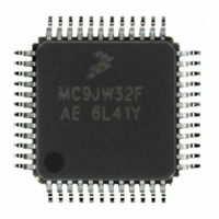
Manufacturer Part Number
MCHC908JW32FAE
Description
IC MCU 32K FLASH 8MHZ 48-LQFP
Manufacturer
Freescale Semiconductor
Series
HC08r
Datasheet
1.RD3152MMA7260Q.pdf
(232 pages)
Specifications of MCHC908JW32FAE
Core Processor
HC08
Core Size
8-Bit
Speed
8MHz
Connectivity
SPI, USB
Peripherals
LED, LVD, POR, PWM
Number Of I /o
29
Program Memory Size
32KB (32K x 8)
Program Memory Type
FLASH
Ram Size
1K x 8
Voltage - Supply (vcc/vdd)
3.5 V ~ 5.5 V
Oscillator Type
Internal
Operating Temperature
0°C ~ 70°C
Package / Case
48-LQFP
Controller Family/series
HC08
No. Of I/o's
48
Ram Memory Size
1KB
Cpu Speed
8MHz
No. Of Timers
1
Embedded Interface Type
SPI
Rohs Compliant
Yes
Processor Series
HC08JW
Core
HC08
Data Bus Width
8 bit
Data Ram Size
1 KB
Interface Type
SPI, USB
Number Of Programmable I/os
29
Number Of Timers
2
Maximum Operating Temperature
+ 70 C
Mounting Style
SMD/SMT
Development Tools By Supplier
FSICEBASE, DEMO908GZ60E, M68EML08GZE, KITUSBSPIDGLEVME, KITUSBSPIEVME, KIT33810EKEVME
Minimum Operating Temperature
0 C
Lead Free Status / RoHS Status
Lead free / RoHS Compliant
Eeprom Size
-
Data Converters
-
Lead Free Status / Rohs Status
Details
Available stocks
Company
Part Number
Manufacturer
Quantity
Price

Company:
Part Number:
MCHC908JW32FAE
Manufacturer:
Freescale Semiconductor
Quantity:
10 000
Part Number:
MCHC908JW32FAE
Manufacturer:
FREESCALE
Quantity:
20 000


Freescale Semiconductor
$001A
$001B
$001C
$001D
$001E
$003D
$003E
$001F
$0020
$003F
$0040
$0041
$0042
$0043
Addr.
to
† One-time writable register after each reset.
Configuration Register 2
IRQ Status and Control
Pullup Control Register
Register Name
Configuration Register
Control Register 1
Control Register 2
Control Register
USB Endpoint 0
USB Endpoint 0
USB Endpoint 0
USB Endpoint 0
Register (ISCR)
Data Register 0
Data Register 1
Data Register 2
Data Register 3
(CONFIG2)
Port Option
Port Option
IRQ Option
(CONFIG)
(PULLCR)
Figure 2-2. Control, Status, and Data Registers (Sheet 3 of 7)
Reserved
Reserved
(POCR1)
(POCR2)
(UE0D0)
(UE0D1)
(UE0D2)
(UE0D3)
(IOCR)
†
Reset:
Reset:
Reset:
Reset:
Reset:
Reset:
Reset:
Reset:
Reset:
Reset:
Reset:
Read:
Read:
Read:
Read:
Read:
Read:
Read:
Read:
Read:
Read:
Read:
Read:
Read:
Write:
Write:
Write:
Write:
Write:
Write:
Write:
Write:
Write:
Write:
Write:
Write:
Write:
UE0D07_OUT UE0D06_OUT UE0D05_OUT UE0D04_OUT UE0D03_OUT UE0D02_OUT UE0D01_OUT UE0D00_OUT
UE0D17_OUT UE0D16_OUT UE0D15_OUT UE0D14_OUT UE0D13_OUT UE0D12_OUT UE0D11_OUT UE0D10_OUT
UE0D27_OUT UE0D26_OUT UE0D25_OUT UE0D24_OUT UE0D23_OUT UE0D22_OUT UE0D21_OUT UE0D20_OUT
UE0D37_OUT UE0D36_OUT UE0D35_OUT UE0D34_OUT UE0D33_OUT UE0D32_OUT UE0D31_OUT UE0D30_OUT
PULL7EN
UE0D07_IN
UE0D17_IN
UE0D27_IN
UE0D37_IN
COPRS
LEDB7
Bit 7
MC68HC908JW32 Data Sheet, Rev. 6
R
R
0
0
0
0
0
0
0
0
0
= Unimplemented
PULL6EN
LVISTOP
UE0D06_IN
UE0D16_IN
UE0D26_IN
UE0D36_IN
LEDB6
R
R
6
0
0
0
0
0
0
0
0
0
PULL5EN
LVIRSTD
UE0D05_IN
UE0D15_IN
UE0D25_IN
UE0D35_IN
PTD7PD
XCLKEN
STOP_
LEDB5
R
R
5
0
0
0
0
0
0
0
0
STOP_RC
Unaffected by reset
Unaffected by reset
Unaffected by reset
Unaffected by reset
LVIPWRD
PULL4EN
UE0D04_IN
UE0D14_IN
UE0D24_IN
UE0D34_IN
PTD3PD
CLKEN
LEDB4
R
R
R
4
0
0
0
0
0
0
0
0
= Reserved
PULL3EN
UE0D03_IN
UE0D13_IN
UE0D23_IN
UE0D33_IN
PTD2PD DPPULLEN
LEDB3
IRQF
R
R
3
0
0
0
0
0
0
0
PULL2EN
UE0D02_IN
UE0D12_IN
UE0D22_IN
UE0D32_IN
PTE3IF
SSREC
LEDB2
ACK
R
R
R
2
0
0
0
0
0
0
0
U = Unaffected by reset
VREG33D
PULL1EN
UE0D01_IN
UE0D11_IN
UE0D21_IN
UE0D31_IN
PTE3IE
PTE3P
LEDB1
IMASK
STOP
R
R
1
0
0
0
0
0
0
Monitor ROM
PULL0EN
UE0D00_IN
UE0D10_IN
UE0D20_IN
UE0D30_IN
URSTD
LEDB0
PTE2P
IRQPD
MODE
COPD
Bit 0
R
R
0
0
0
0
0
0
29
Related parts for MCHC908JW32FAE
Image
Part Number
Description
Manufacturer
Datasheet
Request
R

Part Number:
Description:
Manufacturer:
Freescale Semiconductor, Inc
Datasheet:
Part Number:
Description:
Manufacturer:
Freescale Semiconductor, Inc
Datasheet:
Part Number:
Description:
Manufacturer:
Freescale Semiconductor, Inc
Datasheet:
Part Number:
Description:
Manufacturer:
Freescale Semiconductor, Inc
Datasheet:
Part Number:
Description:
Manufacturer:
Freescale Semiconductor, Inc
Datasheet:
Part Number:
Description:
Manufacturer:
Freescale Semiconductor, Inc
Datasheet:
Part Number:
Description:
Manufacturer:
Freescale Semiconductor, Inc
Datasheet:
Part Number:
Description:
Manufacturer:
Freescale Semiconductor, Inc
Datasheet:
Part Number:
Description:
Manufacturer:
Freescale Semiconductor, Inc
Datasheet:
Part Number:
Description:
Manufacturer:
Freescale Semiconductor, Inc
Datasheet:
Part Number:
Description:
Manufacturer:
Freescale Semiconductor, Inc
Datasheet:
Part Number:
Description:
Manufacturer:
Freescale Semiconductor, Inc
Datasheet:
Part Number:
Description:
Manufacturer:
Freescale Semiconductor, Inc
Datasheet:
Part Number:
Description:
Manufacturer:
Freescale Semiconductor, Inc
Datasheet:
Part Number:
Description:
Manufacturer:
Freescale Semiconductor, Inc
Datasheet: