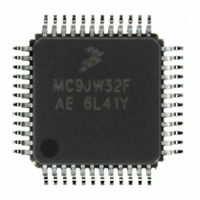
MCHC908JW32FAE Freescale Semiconductor, MCHC908JW32FAE Datasheet - Page 25

MCHC908JW32FAE
Manufacturer Part Number
MCHC908JW32FAE
Description
IC MCU 32K FLASH 8MHZ 48-LQFP
Manufacturer
Freescale Semiconductor
Series
HC08r
Datasheet
1.RD3152MMA7260Q.pdf
(232 pages)
Specifications of MCHC908JW32FAE
Core Processor
HC08
Core Size
8-Bit
Speed
8MHz
Connectivity
SPI, USB
Peripherals
LED, LVD, POR, PWM
Number Of I /o
29
Program Memory Size
32KB (32K x 8)
Program Memory Type
FLASH
Ram Size
1K x 8
Voltage - Supply (vcc/vdd)
3.5 V ~ 5.5 V
Oscillator Type
Internal
Operating Temperature
0°C ~ 70°C
Package / Case
48-LQFP
Controller Family/series
HC08
No. Of I/o's
48
Ram Memory Size
1KB
Cpu Speed
8MHz
No. Of Timers
1
Embedded Interface Type
SPI
Rohs Compliant
Yes
Processor Series
HC08JW
Core
HC08
Data Bus Width
8 bit
Data Ram Size
1 KB
Interface Type
SPI, USB
Number Of Programmable I/os
29
Number Of Timers
2
Maximum Operating Temperature
+ 70 C
Mounting Style
SMD/SMT
Development Tools By Supplier
FSICEBASE, DEMO908GZ60E, M68EML08GZE, KITUSBSPIDGLEVME, KITUSBSPIEVME, KIT33810EKEVME
Minimum Operating Temperature
0 C
Lead Free Status / RoHS Status
Lead free / RoHS Compliant
Eeprom Size
-
Data Converters
-
Lead Free Status / Rohs Status
Details
Available stocks
Company
Part Number
Manufacturer
Quantity
Price
Company:
Part Number:
MCHC908JW32FAE
Manufacturer:
Freescale Semiconductor
Quantity:
10 000
Part Number:
MCHC908JW32FAE
Manufacturer:
FREESCALE
Quantity:
20 000
Chapter 2
Memory
2.1 Introduction
The CPU08 can address 64 Kbytes of memory space. The memory map, shown in
2.2 Input/Output I/O Section
Addresses $0000–$005F, shown in
Additional I/O registers have these addresses:
2.3 Monitor ROM
The 1024 bytes at addresses $FA00–$FDFF and 448 bytes at addresses $FE10–$FFCF are reserved
ROM addresses that contain the instructions for the monitor functions. (See
(MON).)
Freescale Semiconductor
•
•
•
•
•
•
•
•
•
•
•
•
•
•
•
•
•
•
•
•
•
•
•
•
•
•
•
32,768 bytes of user FLASH
1,024 bytes of RAM
64 bytes of USB buffer RAM
48 bytes of user-defined vectors
1,472 bytes of monitor ROM
$1090; PLL control registers, PTCL
$1091; PLL bandwidth control register, PBWC
$1092; PLL multiplier select register high, PMSH
$1093; PLL multiplier select register low, PMSL
$1094; PLL VCO range select register, PMRS
$1095; PLL Reference divider select register, PMDS
$FE00; Break status register, BSR
$FE01; Reset status register, RSR
$FE02; Reserved
$FE03; Break flag control register, BFCR
$FE04; Interrupt status register 1, INT1
$FE05; Interrupt status register 2, INT2
$FE06; Interrupt status register 2, INT3
$FE07; Reserved
$FE08; FLASH control register, FLCR
$FE09; FLASH block protect register, FLBPR
$FE0A; Reserved
$FE0B; Reserved
$FE0C; Break Address Register High, BRKH
$FE0D; Break Address Register Low, BRKL
$FE0E; Break status and control register, BRKSCR
$FFFF; COP control register, COPCTL
MC68HC908JW32 Data Sheet, Rev. 6
Figure
2-2, contain most of the control, status, and data registers.
Chapter 7 Monitor Mode
Figure
2-1, includes:
25


