MCHC908JW32FAE Freescale Semiconductor, MCHC908JW32FAE Datasheet - Page 179
MCHC908JW32FAE
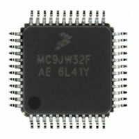
Manufacturer Part Number
MCHC908JW32FAE
Description
IC MCU 32K FLASH 8MHZ 48-LQFP
Manufacturer
Freescale Semiconductor
Series
HC08r
Datasheet
1.RD3152MMA7260Q.pdf
(232 pages)
Specifications of MCHC908JW32FAE
Core Processor
HC08
Core Size
8-Bit
Speed
8MHz
Connectivity
SPI, USB
Peripherals
LED, LVD, POR, PWM
Number Of I /o
29
Program Memory Size
32KB (32K x 8)
Program Memory Type
FLASH
Ram Size
1K x 8
Voltage - Supply (vcc/vdd)
3.5 V ~ 5.5 V
Oscillator Type
Internal
Operating Temperature
0°C ~ 70°C
Package / Case
48-LQFP
Controller Family/series
HC08
No. Of I/o's
48
Ram Memory Size
1KB
Cpu Speed
8MHz
No. Of Timers
1
Embedded Interface Type
SPI
Rohs Compliant
Yes
Processor Series
HC08JW
Core
HC08
Data Bus Width
8 bit
Data Ram Size
1 KB
Interface Type
SPI, USB
Number Of Programmable I/os
29
Number Of Timers
2
Maximum Operating Temperature
+ 70 C
Mounting Style
SMD/SMT
Development Tools By Supplier
FSICEBASE, DEMO908GZ60E, M68EML08GZE, KITUSBSPIDGLEVME, KITUSBSPIEVME, KIT33810EKEVME
Minimum Operating Temperature
0 C
Lead Free Status / RoHS Status
Lead free / RoHS Compliant
Eeprom Size
-
Data Converters
-
Lead Free Status / Rohs Status
Details
Available stocks
Company
Part Number
Manufacturer
Quantity
Price

Company:
Part Number:
MCHC908JW32FAE
Manufacturer:
Freescale Semiconductor
Quantity:
10 000
Part Number:
MCHC908JW32FAE
Manufacturer:
FREESCALE
Quantity:
20 000


Table 13-7
Table 13-8
PTE[7:2] — Port E Data Bits
Freescale Semiconductor
Enable (USBEN)
USB Module
PTE[7:2] are read/write, software-programmable bits. Data direction of each port E pin is under the
control of the corresponding bit in data direction register E.
The PTE3 and PTE2 pullup enable bits, PTE3P and PTE2P, in the port option control register 2
(POCR2) enable 5kΩ pullups to VDD on PTE3 and PTE2 if the USB module is disabled. (See
Port
The PTE2 USB pullup enable bits, DPPULLEN, in the port option control register 2 (POCR2) enable
USB pullups to VREF33 on PTE2 for USB operation. Either of PTE2P or DPPULLEN bit can be
activated at the one time, DPPULLEN bit has higher priority, it will always override the setting of PTE2P
bit.
USB Module
(USBEN)
Enable
1
1
0
0
0
0
0
0
Options.)
1
0
0
0
shows the priority table for PTE2/D+ pin.
shows the priority table for PTE3/D– pin.
PS2 Clock
Generator
(PS2EN)
PTE3 IRQ Enable
Enable
X
X
1
1
0
0
0
0
(PT3IE)
X
1
0
0
Direction
(DDRE2)
Control
Table 13-7. PTE2/D+ Priority Table
Table 13-8. PTE3/D– Priority Table
Data
X
X
X
X
1
1
0
0
MC68HC908JW32 Data Sheet, Rev. 6
Control (DDRE3)
Data Direction
X
X
0
1
5k Pullup
(PTE2P)
Enable
1/0
X
X
X
X
0
1
1
5K Pullup Enable
(PTE3P)
(DPPULPEN)
0/1
0/1
0/1
X
USB D+
Enable
Pullup
1/0
1
0
0
1
0
1
0
USB D– pin
GPIO input with associated interrupt
function and optional 5k pullup to VDD
GPIO input with optional 5k pullup to
VDD
GPIO output (open-drain) with optional
5k pullup to VDD
D+ with pullup to VREF33.
D+ without pullup
PS2 Clock output (open-drain) with
optional 5k pullup to VDD
PS2 Clock output (open-drain) with
optional 1.2k pullup to VREG33
GPIO output (open-drain) with 1.2K
pullup to REG33V
GPIO output (open-drain) with 5k
pullup to VDD
GPIO input with 1.2K pullup to
REG33V
GPIO input with 5K pullup to VDD
Pin Function
Pin Function
13.7
Port E
179
Related parts for MCHC908JW32FAE
Image
Part Number
Description
Manufacturer
Datasheet
Request
R

Part Number:
Description:
Manufacturer:
Freescale Semiconductor, Inc
Datasheet:
Part Number:
Description:
Manufacturer:
Freescale Semiconductor, Inc
Datasheet:
Part Number:
Description:
Manufacturer:
Freescale Semiconductor, Inc
Datasheet:
Part Number:
Description:
Manufacturer:
Freescale Semiconductor, Inc
Datasheet:
Part Number:
Description:
Manufacturer:
Freescale Semiconductor, Inc
Datasheet:
Part Number:
Description:
Manufacturer:
Freescale Semiconductor, Inc
Datasheet:
Part Number:
Description:
Manufacturer:
Freescale Semiconductor, Inc
Datasheet:
Part Number:
Description:
Manufacturer:
Freescale Semiconductor, Inc
Datasheet:
Part Number:
Description:
Manufacturer:
Freescale Semiconductor, Inc
Datasheet:
Part Number:
Description:
Manufacturer:
Freescale Semiconductor, Inc
Datasheet:
Part Number:
Description:
Manufacturer:
Freescale Semiconductor, Inc
Datasheet:
Part Number:
Description:
Manufacturer:
Freescale Semiconductor, Inc
Datasheet:
Part Number:
Description:
Manufacturer:
Freescale Semiconductor, Inc
Datasheet:
Part Number:
Description:
Manufacturer:
Freescale Semiconductor, Inc
Datasheet:
Part Number:
Description:
Manufacturer:
Freescale Semiconductor, Inc
Datasheet: