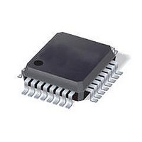
ST7FOXK1T6TR STMicroelectronics, ST7FOXK1T6TR Datasheet - Page 97

ST7FOXK1T6TR
Manufacturer Part Number
ST7FOXK1T6TR
Description
IC MCU 8BIT 4K FLASH 20LQFP
Manufacturer
STMicroelectronics
Series
ST7r
Datasheet
1.ST7FOXF1M6.pdf
(226 pages)
Specifications of ST7FOXK1T6TR
Core Processor
ST7
Core Size
8-Bit
Speed
8MHz
Connectivity
I²C
Peripherals
LVD, POR, PWM, WDT
Number Of I /o
24
Program Memory Size
4KB (4K x 8)
Program Memory Type
FLASH
Ram Size
384 x 8
Voltage - Supply (vcc/vdd)
4.5 V ~ 5.5 V
Data Converters
A/D 10x10b
Oscillator Type
Internal
Operating Temperature
-40°C ~ 85°C
Package / Case
32-LQFP
Processor Series
ST7FOXx
Core
ST7
Data Bus Width
8 bit
Data Ram Size
384 B
Interface Type
I2C
Maximum Clock Frequency
8 MHz
Number Of Programmable I/os
24
Number Of Timers
4
Maximum Operating Temperature
+ 85 C
Mounting Style
SMD/SMT
Development Tools By Supplier
ST7FLITE-SK/RAIS, STX-RLINK
Minimum Operating Temperature
- 40 C
On-chip Adc
10 bit, 1 Channel
For Use With
497-5049 - KIT STARTER RAISONANCE ST7FLITE
Lead Free Status / RoHS Status
Lead free / RoHS Compliant
Eeprom Size
-
Lead Free Status / Rohs Status
Details
Available stocks
Company
Part Number
Manufacturer
Quantity
Price
Company:
Part Number:
ST7FOXK1T6TR
Manufacturer:
STMicroelectronics
Quantity:
10 000
- Current page: 97 of 226
- Download datasheet (4Mb)
ST7FOXF1, ST7FOXK1, ST7FOXK2
10.2.4
10.2.5
Note:
Force update
In order not to wait for the counter
programmable counter
which when set, make the counters start with the overflow value, i.e. FFFh. After overflow,
the counters start counting from their respective auto reload register values.
These bits are FORCE1 and FORCE2 in the ATCSR2 register. FORCE1 is used to force an
overflow on Counter 1 and, FORCE2 is used for Counter 2. These bits are set by software
and reset by hardware after the respective counter overflow event has occurred.
This feature can be used at any time. All related features such as PWM generation, Output
Compare, Input Capture, One-pulse (refer to
pulse
Figure 51. Force overflow timing diagram
Low power modes
Table 35.
Interrupts
Table 36.
The AT4 IC is connected to an interrupt vector. The OVF event is mapped on a separate
vector (see Interrupts chapter).
They generate an interrupt if the enable bit is set in the ATCSR register and the interrupt
mask in the CC register is reset (RIM instruction).
FORCE2 FORCE1
Overflow Event2
Interrupt Event
Overflow Event
AT4 IC Event
mode) etc. can be used this way.
Mode
Wait
FORCEx
Halt
CNTRx
f
CNTRx
Effect of low power modes on autoreload timer
Description of interrupt events
ATCSR2 register
E03
x
overflow is provided. For both counters, a separate bit is provided
E04
Event
OVF1
OVF2
Flag
ICF
FFF
x
overflow to load the value into active DCRx registers, a
Control bit
Enable
ARRx
OVIE1
OVIE2
ICIE
Figure 50: Dynamic DCR2/3 update in one
No effect on AT timer
AT timer halted.
Description
Exit from
Wait
Yes
Yes
Yes
Exit from
Halt
No
No
No
On-chip peripherals
Active-Halt
Exit from
Yes
No
No
97/226
Related parts for ST7FOXK1T6TR
Image
Part Number
Description
Manufacturer
Datasheet
Request
R

Part Number:
Description:
Low cost flash 8bit micro
Manufacturer:
STMicroelectronics
Datasheet:

Part Number:
Description:
STMicroelectronics [RIPPLE-CARRY BINARY COUNTER/DIVIDERS]
Manufacturer:
STMicroelectronics
Datasheet:

Part Number:
Description:
STMicroelectronics [LIQUID-CRYSTAL DISPLAY DRIVERS]
Manufacturer:
STMicroelectronics
Datasheet:

Part Number:
Description:
BOARD EVAL FOR MEMS SENSORS
Manufacturer:
STMicroelectronics
Datasheet:

Part Number:
Description:
NPN TRANSISTOR POWER MODULE
Manufacturer:
STMicroelectronics
Datasheet:

Part Number:
Description:
TURBOSWITCH ULTRA-FAST HIGH VOLTAGE DIODE
Manufacturer:
STMicroelectronics
Datasheet:

Part Number:
Description:
Manufacturer:
STMicroelectronics
Datasheet:

Part Number:
Description:
DIODE / SCR MODULE
Manufacturer:
STMicroelectronics
Datasheet:

Part Number:
Description:
DIODE / SCR MODULE
Manufacturer:
STMicroelectronics
Datasheet:

Part Number:
Description:
Search -----> STE16N100
Manufacturer:
STMicroelectronics
Datasheet:

Part Number:
Description:
Search ---> STE53NA50
Manufacturer:
STMicroelectronics
Datasheet:

Part Number:
Description:
NPN Transistor Power Module
Manufacturer:
STMicroelectronics
Datasheet:


