ST7FOXK1T6TR STMicroelectronics, ST7FOXK1T6TR Datasheet - Page 12
ST7FOXK1T6TR
Manufacturer Part Number
ST7FOXK1T6TR
Description
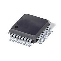
IC MCU 8BIT 4K FLASH 20LQFP
Manufacturer
STMicroelectronics
Series
ST7r
Datasheet
1.ST7FOXF1M6.pdf
(226 pages)
Specifications of ST7FOXK1T6TR
Core Processor
ST7
Core Size
8-Bit
Speed
8MHz
Connectivity
I²C
Peripherals
LVD, POR, PWM, WDT
Number Of I /o
24
Program Memory Size
4KB (4K x 8)
Program Memory Type
FLASH
Ram Size
384 x 8
Voltage - Supply (vcc/vdd)
4.5 V ~ 5.5 V
Data Converters
A/D 10x10b
Oscillator Type
Internal
Operating Temperature
-40°C ~ 85°C
Package / Case
32-LQFP
Processor Series
ST7FOXx
Core
ST7
Data Bus Width
8 bit
Data Ram Size
384 B
Interface Type
I2C
Maximum Clock Frequency
8 MHz
Number Of Programmable I/os
24
Number Of Timers
4
Maximum Operating Temperature
+ 85 C
Mounting Style
SMD/SMT
Development Tools By Supplier
ST7FLITE-SK/RAIS, STX-RLINK
Minimum Operating Temperature
- 40 C
On-chip Adc
10 bit, 1 Channel
For Use With
497-5049 - KIT STARTER RAISONANCE ST7FLITE
Lead Free Status / RoHS Status
Lead free / RoHS Compliant
Eeprom Size
-
Lead Free Status / Rohs Status
Details
Available stocks
Company
Part Number
Manufacturer
Quantity
Price
Company:

Part Number:
ST7FOXK1T6TR
Manufacturer:
STMicroelectronics
Quantity:
10 000


List of figures
Figure 49.
Figure 50.
Figure 51.
Figure 52.
Figure 53.
Figure 54.
Figure 55.
Figure 56.
Figure 57.
Figure 58.
Figure 59.
Figure 60.
Figure 61.
Figure 62.
Figure 63.
Figure 64.
Figure 65.
Figure 66.
Figure 67.
Figure 68.
Figure 69.
Figure 70.
Figure 71.
Figure 72.
Figure 73.
Figure 74.
Figure 75.
Figure 76.
Figure 77.
Figure 78.
Figure 79.
Figure 80.
Figure 81.
Figure 82.
Figure 83.
Figure 84.
Figure 85.
Figure 86.
Figure 87.
Figure 88.
Figure 89.
Figure 90.
Figure 91.
Figure 92.
Figure 93.
Figure 94.
Figure 95.
Figure 96.
Figure 97.
12/226
One pulse mode and PWM timing diagram . . . . . . . . . . . . . . . . . . . . . . . . . . . . . . . . . . . . 95
Dynamic DCR2/3 update in one pulse mode . . . . . . . . . . . . . . . . . . . . . . . . . . . . . . . . . . . 96
Force overflow timing diagram . . . . . . . . . . . . . . . . . . . . . . . . . . . . . . . . . . . . . . . . . . . . . . 97
Lite timer 2 block diagram . . . . . . . . . . . . . . . . . . . . . . . . . . . . . . . . . . . . . . . . . . . . . . . . 111
Input Capture timing diagram . . . . . . . . . . . . . . . . . . . . . . . . . . . . . . . . . . . . . . . . . . . . . . 112
Watchdog timing diagram . . . . . . . . . . . . . . . . . . . . . . . . . . . . . . . . . . . . . . . . . . . . . . . . . 113
Timer block diagram . . . . . . . . . . . . . . . . . . . . . . . . . . . . . . . . . . . . . . . . . . . . . . . . . . . . . 119
16-bit read sequence . . . . . . . . . . . . . . . . . . . . . . . . . . . . . . . . . . . . . . . . . . . . . . . . . . . . 120
Counter timing diagram, internal clock divided by 2 . . . . . . . . . . . . . . . . . . . . . . . . . . . . . 121
Counter timing diagram, internal clock divided by 4 . . . . . . . . . . . . . . . . . . . . . . . . . . . . . 121
Counter timing diagram, internal clock divided by 8 . . . . . . . . . . . . . . . . . . . . . . . . . . . . . 121
Input capture block diagram . . . . . . . . . . . . . . . . . . . . . . . . . . . . . . . . . . . . . . . . . . . . . . . 123
Input capture timing diagram . . . . . . . . . . . . . . . . . . . . . . . . . . . . . . . . . . . . . . . . . . . . . . 123
Output compare block diagram . . . . . . . . . . . . . . . . . . . . . . . . . . . . . . . . . . . . . . . . . . . . 126
Output compare timing diagram, f
Output compare timing diagram, f
One pulse mode sequence . . . . . . . . . . . . . . . . . . . . . . . . . . . . . . . . . . . . . . . . . . . . . . . . 128
One pulse mode timing example . . . . . . . . . . . . . . . . . . . . . . . . . . . . . . . . . . . . . . . . . . . 129
Pulse width modulation mode timing example . . . . . . . . . . . . . . . . . . . . . . . . . . . . . . . . . 129
Pulse width modulation cycle . . . . . . . . . . . . . . . . . . . . . . . . . . . . . . . . . . . . . . . . . . . . . . 130
I
I
Transfer sequencing . . . . . . . . . . . . . . . . . . . . . . . . . . . . . . . . . . . . . . . . . . . . . . . . . . . . . 148
Event flags and interrupt generation . . . . . . . . . . . . . . . . . . . . . . . . . . . . . . . . . . . . . . . . . 149
Serial peripheral interface block diagram . . . . . . . . . . . . . . . . . . . . . . . . . . . . . . . . . . . . . 159
Single master/ single slave application . . . . . . . . . . . . . . . . . . . . . . . . . . . . . . . . . . . . . . . 160
Generic SS timing diagram . . . . . . . . . . . . . . . . . . . . . . . . . . . . . . . . . . . . . . . . . . . . . . . . 161
Hardware/software slave select management . . . . . . . . . . . . . . . . . . . . . . . . . . . . . . . . . 161
Data clock timing diagram . . . . . . . . . . . . . . . . . . . . . . . . . . . . . . . . . . . . . . . . . . . . . . . . 164
Clearing the WCOL bit (write collision flag) software sequence . . . . . . . . . . . . . . . . . . . . 166
Single master / multiple slave configuration . . . . . . . . . . . . . . . . . . . . . . . . . . . . . . . . . . . 167
ADC block diagram . . . . . . . . . . . . . . . . . . . . . . . . . . . . . . . . . . . . . . . . . . . . . . . . . . . . . . 174
Pin loading conditions . . . . . . . . . . . . . . . . . . . . . . . . . . . . . . . . . . . . . . . . . . . . . . . . . . . . 187
Pin input voltage . . . . . . . . . . . . . . . . . . . . . . . . . . . . . . . . . . . . . . . . . . . . . . . . . . . . . . . . 188
SPI slave timing diagram with CPHA=0 . . . . . . . . . . . . . . . . . . . . . . . . . . . . . . . . . . . . . . 196
SPI slave timing diagram with CPHA=1 . . . . . . . . . . . . . . . . . . . . . . . . . . . . . . . . . . . . . . 196
SPI master timing diagram . . . . . . . . . . . . . . . . . . . . . . . . . . . . . . . . . . . . . . . . . . . . . . . . 197
Typical application with an external clock source . . . . . . . . . . . . . . . . . . . . . . . . . . . . . . . 198
Typical application with a crystal or ceramic resonator. . . . . . . . . . . . . . . . . . . . . . . . . . . 199
Two typical applications with unused I/O pin . . . . . . . . . . . . . . . . . . . . . . . . . . . . . . . . . . 204
RESET pin protection when LVD is enabled . . . . . . . . . . . . . . . . . . . . . . . . . . . . . . . . . . 207
RESET pin protection when LVD is disabled . . . . . . . . . . . . . . . . . . . . . . . . . . . . . . . . . . 208
Typical application with ADC . . . . . . . . . . . . . . . . . . . . . . . . . . . . . . . . . . . . . . . . . . . . . . 209
ADC accuracy characteristics . . . . . . . . . . . . . . . . . . . . . . . . . . . . . . . . . . . . . . . . . . . . . . 210
ST7FOXF1/ST7FOXK1/ST7FOXK2 ordering information scheme . . . . . . . . . . . . . . . . . 214
20-pin plastic small outline package, 300-mil width, package outline. . . . . . . . . . . . . . . . 220
20-pin plastic dual in-line package, 300-mil width, package outline . . . . . . . . . . . . . . . . . 221
32-pin plastic dual in-line package, shrink 400-mil width, package outline. . . . . . . . . . . . 222
32-pin low profile quad flat package (7x7), package outline . . . . . . . . . . . . . . . . . . . . . . . 223
2
2
C bus protocol . . . . . . . . . . . . . . . . . . . . . . . . . . . . . . . . . . . . . . . . . . . . . . . . . . . . . . . . 142
C interface block diagram . . . . . . . . . . . . . . . . . . . . . . . . . . . . . . . . . . . . . . . . . . . . . . . 143
TIMER
TIMER
= f
= f
CPU
CPU
/2 . . . . . . . . . . . . . . . . . . . . . . . . . . . . . . . 126
/4 . . . . . . . . . . . . . . . . . . . . . . . . . . . . . . . 127
ST7FOXF1, ST7FOXK1, ST7FOXK2
Related parts for ST7FOXK1T6TR
Image
Part Number
Description
Manufacturer
Datasheet
Request
R

Part Number:
Description:
Low cost flash 8bit micro
Manufacturer:
STMicroelectronics
Datasheet:
Part Number:
Description:
STMicroelectronics [RIPPLE-CARRY BINARY COUNTER/DIVIDERS]
Manufacturer:
STMicroelectronics
Datasheet:
Part Number:
Description:
STMicroelectronics [LIQUID-CRYSTAL DISPLAY DRIVERS]
Manufacturer:
STMicroelectronics
Datasheet:

Part Number:
Description:
BOARD EVAL FOR MEMS SENSORS
Manufacturer:
STMicroelectronics
Datasheet:
Part Number:
Description:
NPN TRANSISTOR POWER MODULE
Manufacturer:
STMicroelectronics
Datasheet:
Part Number:
Description:
TURBOSWITCH ULTRA-FAST HIGH VOLTAGE DIODE
Manufacturer:
STMicroelectronics
Datasheet:
Part Number:
Description:
Manufacturer:
STMicroelectronics
Datasheet:
Part Number:
Description:
DIODE / SCR MODULE
Manufacturer:
STMicroelectronics
Datasheet:
Part Number:
Description:
DIODE / SCR MODULE
Manufacturer:
STMicroelectronics
Datasheet:
Part Number:
Description:
Search -----> STE16N100
Manufacturer:
STMicroelectronics
Datasheet:
Part Number:
Description:
Search ---> STE53NA50
Manufacturer:
STMicroelectronics
Datasheet:
Part Number:
Description:
NPN Transistor Power Module
Manufacturer:
STMicroelectronics
Datasheet: