P89LPC9408FBD,557 NXP Semiconductors, P89LPC9408FBD,557 Datasheet - Page 8
P89LPC9408FBD,557
Manufacturer Part Number
P89LPC9408FBD,557
Description
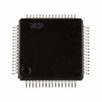
IC 80C51 MCU FLASH 8K 64-LQFP
Manufacturer
NXP Semiconductors
Series
LPC900r
Datasheet
1.P89LPC9408FBD557.pdf
(69 pages)
Specifications of P89LPC9408FBD,557
Program Memory Type
FLASH
Program Memory Size
8KB (8K x 8)
Package / Case
64-LQFP
Core Processor
8051
Core Size
8-Bit
Speed
18MHz
Connectivity
I²C, SPI, UART/USART
Peripherals
Brown-out Detect/Reset, LCD, LED, POR, PWM, WDT
Number Of I /o
23
Eeprom Size
512 x 8
Ram Size
256 x 8
Voltage - Supply (vcc/vdd)
2.4 V ~ 3.6 V
Data Converters
A/D 8x10b
Oscillator Type
Internal
Operating Temperature
-40°C ~ 85°C
Processor Series
P89LPC9x
Core
80C51
Data Bus Width
8 bit
Data Ram Size
256 B
Interface Type
I2C/SPI/UART
Maximum Clock Frequency
18 MHz
Number Of Programmable I/os
23
Number Of Timers
2
Operating Supply Voltage
2.4 V to 3.6 V
Maximum Operating Temperature
+ 85 C
Mounting Style
SMD/SMT
3rd Party Development Tools
PK51, CA51, A51, ULINK2
Minimum Operating Temperature
- 40 C
On-chip Adc
8-ch x 10-bit
Lead Free Status / RoHS Status
Lead free / RoHS Compliant
For Use With
OM10097 - KIT FOR LCD DEMO LPC9408EPM900K - EMULATOR/PROGRAMMER NXP P89LPC9568-4000 - DEMO BOARD SPI/I2C TO DUAL UART568-3510 - DEMO BOARD SPI/I2C TO UART568-1759 - EMULATOR DEBUGGER/PROGRMMR LPC9X
Lead Free Status / Rohs Status
Lead free / RoHS Compliant
Other names
568-3228
935280583557
P89LPC9408FBD
935280583557
P89LPC9408FBD
Available stocks
Company
Part Number
Manufacturer
Quantity
Price
Company:

Part Number:
P89LPC9408FBD,557
Manufacturer:
NXP Semiconductors
Quantity:
10 000


Philips Semiconductors
Table 3:
P89LPC9408_1
Product data sheet
Symbol
P1.2/T0/SCL
P1.3/INT0/
SDA
P1.4/INT1
P1.5/RST
P1.6/OCB
P1.7/OCC/
AD04
P2.0 to P2.3,
P2.5
P2.0/ICB/
AD07
P2.1/OCD/
AD06
P2.2/MOSI
P2.3/MISO
Pin description
Pin
17
16
15
11
10
9
6
7
18
19
…continued
Type Description
I/O
I/O
I/O
I/O
I
I/O
I
I
I
I
I/O
O
I/O
O
I
I/O
I/O
I
I
I/O
O
I
I/O
I/O
I/O
I/O
P1.2 — Port 1 bit 2 (open-drain when used as output).
T0 — Timer/counter 0 external count input or overflow output (open-drain when used
as output).
SCL — I
P1.3 — Port 1 bit 3 (open-drain when used as output).
INT0 — External interrupt 0 input.
SDA — I
P1.4 — Port 1 bit 4.
INT1 — External interrupt 1 input.
P1.5 — Port 1 bit 5 (input only).
RST — External Reset input during power-on or if selected via UCFG1. When
functioning as a reset input, a LOW on this pin resets the microcontroller, causing I/O
ports and peripherals to take on their default states, and the processor begins
execution at address 0. Also used during a power-on sequence to force ISP mode.
When using an oscillator frequency above 12 MHz, the reset input function of
P1.5 must be enabled. An external circuit is required to hold the device in reset at
power-up until V
removed V
using an oscillator frequency above 12 MHz, in some applications, an external
brownout detect circuit may be required to hold the device in reset when V
below the minimum specified operating range.
P1.6 — Port 1 bit 6.
OCB — Output Compare B.
P1.7 — Port 1 bit 7.
OCC — Output Compare C.
AD04 — ADC0 channel 4 analog input.
Port 2: Port 2 is an 5-bit I/O port with a user-configurable output type. During reset
Port 2 latches are configured in the input only mode with the internal pull-up disabled.
The operation of Port 2 pins as inputs and outputs depends upon the port configuration
selected. Each port pin is configured independently. Refer to
configurations”
All pins have Schmitt trigger inputs.
Port 2 also provides various special functions as described below:
P2.0 — Port 2 bit 0.
ICB — Input Capture B.
AD07 — ADC0 channel 7 analog input.
P2.1 — Port 2 bit 1.
OCD — Output Compare D.
AD06 — ADC0 channel 6 analog input.
P2.2 — Port 2 bit 2.
MOSI — SPI master out slave in. When configured as master, this pin is output; when
configured as slave, this pin is input.
P2.3 — Port 2 bit 3.
MISO — When configured as master, this pin is input, when configured as slave, this
pin is output.
8-bit two-clock 80C51 core with 32 segment
2
2
C-bus serial clock input/output.
C-bus serial data input/output.
DD
Rev. 01 — 16 December 2005
will fall below the minimum specified operating voltage. When
and
DD
Table 12 “Static electrical characteristics”
has reached its specified level. When system power is
© Koninklijke Philips Electronics N.V. 2005. All rights reserved.
P89LPC9408
4 LCD driver, 10-bit ADC
Section 7.13.1 “Port
for details.
DD
8 of 69
falls
Related parts for P89LPC9408FBD,557
Image
Part Number
Description
Manufacturer
Datasheet
Request
R

Part Number:
Description:
8-bit Microcontroller With Two-clock 80c51 Core 8 Kb 3 V Byte-erasable Flash, 32 Segment X 4 Lcd Driver, 10-bit Adc
Manufacturer:
NXP Semiconductors
Datasheet:
Part Number:
Description:
NXP Semiconductors designed the LPC2420/2460 microcontroller around a 16-bit/32-bitARM7TDMI-S CPU core with real-time debug interfaces that include both JTAG andembedded trace
Manufacturer:
NXP Semiconductors
Datasheet:

Part Number:
Description:
NXP Semiconductors designed the LPC2458 microcontroller around a 16-bit/32-bitARM7TDMI-S CPU core with real-time debug interfaces that include both JTAG andembedded trace
Manufacturer:
NXP Semiconductors
Datasheet:
Part Number:
Description:
NXP Semiconductors designed the LPC2468 microcontroller around a 16-bit/32-bitARM7TDMI-S CPU core with real-time debug interfaces that include both JTAG andembedded trace
Manufacturer:
NXP Semiconductors
Datasheet:
Part Number:
Description:
NXP Semiconductors designed the LPC2470 microcontroller, powered by theARM7TDMI-S core, to be a highly integrated microcontroller for a wide range ofapplications that require advanced communications and high quality graphic displays
Manufacturer:
NXP Semiconductors
Datasheet:
Part Number:
Description:
NXP Semiconductors designed the LPC2478 microcontroller, powered by theARM7TDMI-S core, to be a highly integrated microcontroller for a wide range ofapplications that require advanced communications and high quality graphic displays
Manufacturer:
NXP Semiconductors
Datasheet:
Part Number:
Description:
The Philips Semiconductors XA (eXtended Architecture) family of 16-bit single-chip microcontrollers is powerful enough to easily handle the requirements of high performance embedded applications, yet inexpensive enough to compete in the market for hi
Manufacturer:
NXP Semiconductors
Datasheet:
Part Number:
Description:
The XA-S3 device is a member of Philips Semiconductors? XA(eXtended Architecture) family of high performance 16-bitsingle-chip microcontrollers
Manufacturer:
NXP Semiconductors
Datasheet:

Part Number:
Description:
The NXP BlueStreak LH75401/LH75411 family consists of two low-cost 16/32-bit System-on-Chip (SoC) devices
Manufacturer:
NXP Semiconductors
Datasheet:
Part Number:
Description:
The NXP LPC3130/3131 combine an 180 MHz ARM926EJ-S CPU core, high-speed USB2
Manufacturer:
NXP Semiconductors
Datasheet:
Part Number:
Description:
The NXP LPC3141 combine a 270 MHz ARM926EJ-S CPU core, High-speed USB 2
Manufacturer:
NXP Semiconductors
Part Number:
Description:
The NXP LPC3143 combine a 270 MHz ARM926EJ-S CPU core, High-speed USB 2
Manufacturer:
NXP Semiconductors

Part Number:
Description:
The NXP LPC3152 combines an 180 MHz ARM926EJ-S CPU core, High-speed USB 2
Manufacturer:
NXP Semiconductors
Part Number:
Description:
The NXP LPC3154 combines an 180 MHz ARM926EJ-S CPU core, High-speed USB 2
Manufacturer:
NXP Semiconductors