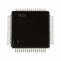
P89LPC9408FBD,557 NXP Semiconductors, P89LPC9408FBD,557 Datasheet - Page 50

P89LPC9408FBD,557
Manufacturer Part Number
P89LPC9408FBD,557
Description
IC 80C51 MCU FLASH 8K 64-LQFP
Manufacturer
NXP Semiconductors
Series
LPC900r
Datasheet
1.P89LPC9408FBD557.pdf
(69 pages)
Specifications of P89LPC9408FBD,557
Program Memory Type
FLASH
Program Memory Size
8KB (8K x 8)
Package / Case
64-LQFP
Core Processor
8051
Core Size
8-Bit
Speed
18MHz
Connectivity
I²C, SPI, UART/USART
Peripherals
Brown-out Detect/Reset, LCD, LED, POR, PWM, WDT
Number Of I /o
23
Eeprom Size
512 x 8
Ram Size
256 x 8
Voltage - Supply (vcc/vdd)
2.4 V ~ 3.6 V
Data Converters
A/D 8x10b
Oscillator Type
Internal
Operating Temperature
-40°C ~ 85°C
Processor Series
P89LPC9x
Core
80C51
Data Bus Width
8 bit
Data Ram Size
256 B
Interface Type
I2C/SPI/UART
Maximum Clock Frequency
18 MHz
Number Of Programmable I/os
23
Number Of Timers
2
Operating Supply Voltage
2.4 V to 3.6 V
Maximum Operating Temperature
+ 85 C
Mounting Style
SMD/SMT
3rd Party Development Tools
PK51, CA51, A51, ULINK2
Minimum Operating Temperature
- 40 C
On-chip Adc
8-ch x 10-bit
Lead Free Status / RoHS Status
Lead free / RoHS Compliant
For Use With
OM10097 - KIT FOR LCD DEMO LPC9408EPM900K - EMULATOR/PROGRAMMER NXP P89LPC9568-4000 - DEMO BOARD SPI/I2C TO DUAL UART568-3510 - DEMO BOARD SPI/I2C TO UART568-1759 - EMULATOR DEBUGGER/PROGRMMR LPC9X
Lead Free Status / Rohs Status
Lead free / RoHS Compliant
Other names
568-3228
935280583557
P89LPC9408FBD
935280583557
P89LPC9408FBD
Available stocks
Company
Part Number
Manufacturer
Quantity
Price
Company:
Part Number:
P89LPC9408FBD,557
Manufacturer:
NXP Semiconductors
Quantity:
10 000
Philips Semiconductors
8. ADC
P89LPC9408_1
Product data sheet
8.1 General description
8.2 Features
8.3 Block diagram
The P89LPC9408 has a 10-bit, 8-channel multiplexed successive approximation
analog-to-digital converter module. A block diagram of the ADC is shown in
The ADC consists of an 8-input multiplexer which feeds a sample-and-hold circuit
providing an input signal to one of two comparator inputs. The control logic in combination
with the SAR drives a digital-to-analog converter which provides the other input to the
comparator. The output of the comparator is fed to the SAR.
Fig 21. ADC block diagram
10-bit, 8-channel multiplexed input, successive approximation ADC.
Eight result register pairs.
Six operating modes
Three conversion start modes
10-bit conversion time of 4 s at an ADC clock of 9 MHz
Interrupt or polled operation
High and Low Boundary limits interrupt; selectable in or out-of-range
Clock divider
Power-down mode
Fixed channel, single conversion mode
Fixed channel, continuous conversion mode
Auto scan, single conversion mode
Auto scan, continuous conversion mode
Dual channel, continuous conversion mode
Single step mode
Timer triggered start
Start immediately
Edge triggered
8-bit two-clock 80C51 core with 32 segment
INPUT
MUX
Rev. 01 — 16 December 2005
comp
+
–
DAC0
CCLK
© Koninklijke Philips Electronics N.V. 2005. All rights reserved.
SAR
P89LPC9408
4 LCD driver, 10-bit ADC
8
CONTROL
LOGIC
002aab103
Figure
21.
50 of 69


