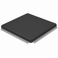
AT32UC3A0512-ALTTA Atmel, AT32UC3A0512-ALTTA Datasheet - Page 390

AT32UC3A0512-ALTTA
Manufacturer Part Number
AT32UC3A0512-ALTTA
Description
IC MCU AVR32 512K FLASH 144LQFP
Manufacturer
Atmel
Series
AVR®32 UC3r
Datasheet
1.ATEVK1104.pdf
(826 pages)
Specifications of AT32UC3A0512-ALTTA
Core Processor
AVR
Core Size
32-Bit
Speed
66MHz
Connectivity
EBI/EMI, Ethernet, I²C, SPI, SSC, UART/USART, USB OTG
Peripherals
Brown-out Detect/Reset, POR, PWM, WDT
Number Of I /o
109
Program Memory Size
512KB (512K x 8)
Program Memory Type
FLASH
Ram Size
64K x 8
Voltage - Supply (vcc/vdd)
1.65 V ~ 1.95 V
Data Converters
A/D 8x10b
Oscillator Type
Internal
Operating Temperature
-40°C ~ 85°C
Package / Case
144-LQFP
Lead Free Status / RoHS Status
Lead free / RoHS Compliant
Eeprom Size
-
Available stocks
Company
Part Number
Manufacturer
Quantity
Price
- Current page: 390 of 826
- Download datasheet (20Mb)
27.6.6.2
Figure 27-23. TDF Optimization: No TDF wait states are inserted if the TDF period is over when the next access begins
27.6.6.3
32058J–AVR32–04/11
CLK_SMC
D[15:0]
A[25:2]
NCS0
NWE
NRD
TDF Optimization Enabled (TDF_MODE = 1)
TDF Optimization Disabled (TDF_MODE = 0)
Read access on NCS0 (NRD controlled)
When the TDF_MODE of the MODE register is set to 1 (TDF optimization is enabled), the SMC
takes advantage of the setup period of the next access to optimize the number of wait states
cycle to insert.
Figure 27-23
NWE, on Chip Select 0. Chip Select 0 has been programmed with:
NRD_HOLD = 4; READ_MODE = 1 (NRD controlled)
NWE_SETUP = 3; WRITE_MODE = 1 (NWE controlled)
TDF_CYCLES = 6; TDF_MODE = 1 (optimization enabled).
When optimization is disabled, tdf wait states are inserted at the end of the read transfer, so that
the data float period is ended when the second access begins. If the hold period of the read1
controlling signal overlaps the data float period, no additional tdf wait states will be inserted.
Figure
• read access followed by a read access on another chip select,
• read access followed by a write access on another chip select,
27-24,
shows a read access controlled by NRD, followed by a write access controlled by
NRD_HOLD = 4
Figure 27-25
TDF_CYCLES = 6
and
Figure 27-26
Read to Write
Wait State
NWE_SETUP = 3
illustrate the cases:
write access on NCS0 (NWE controlled)
AT32UC3A
390
Related parts for AT32UC3A0512-ALTTA
Image
Part Number
Description
Manufacturer
Datasheet
Request
R

Part Number:
Description:
MCU, MPU & DSP Development Tools KICKSTART KIT FOR AT32UC3A
Manufacturer:
IAR Systems

Part Number:
Description:
DEV KIT FOR AVR/AVR32
Manufacturer:
Atmel
Datasheet:

Part Number:
Description:
INTERVAL AND WIPE/WASH WIPER CONTROL IC WITH DELAY
Manufacturer:
ATMEL Corporation
Datasheet:

Part Number:
Description:
Low-Voltage Voice-Switched IC for Hands-Free Operation
Manufacturer:
ATMEL Corporation
Datasheet:

Part Number:
Description:
MONOLITHIC INTEGRATED FEATUREPHONE CIRCUIT
Manufacturer:
ATMEL Corporation
Datasheet:

Part Number:
Description:
AM-FM Receiver IC U4255BM-M
Manufacturer:
ATMEL Corporation
Datasheet:

Part Number:
Description:
Monolithic Integrated Feature Phone Circuit
Manufacturer:
ATMEL Corporation
Datasheet:

Part Number:
Description:
Multistandard Video-IF and Quasi Parallel Sound Processing
Manufacturer:
ATMEL Corporation
Datasheet:

Part Number:
Description:
High-performance EE PLD
Manufacturer:
ATMEL Corporation
Datasheet:

Part Number:
Description:
8-bit Flash Microcontroller
Manufacturer:
ATMEL Corporation
Datasheet:

Part Number:
Description:
2-Wire Serial EEPROM
Manufacturer:
ATMEL Corporation
Datasheet:


