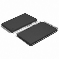
AT91SAM7SE32-AU Atmel, AT91SAM7SE32-AU Datasheet - Page 646

AT91SAM7SE32-AU
Manufacturer Part Number
AT91SAM7SE32-AU
Description
MCU ARM 32K HS FLASH 128-LQFP
Manufacturer
Atmel
Series
AT91SAMr
Specifications of AT91SAM7SE32-AU
Core Processor
ARM7
Core Size
16/32-Bit
Speed
55MHz
Connectivity
EBI/EMI, I²C, SPI, SSC, UART/USART, USB
Peripherals
Brown-out Detect/Reset, POR, PWM, WDT
Number Of I /o
88
Program Memory Size
32KB (32K x 8)
Program Memory Type
FLASH
Ram Size
8K x 8
Voltage - Supply (vcc/vdd)
1.65 V ~ 1.95 V
Data Converters
A/D 8x10b
Oscillator Type
Internal
Operating Temperature
-40°C ~ 85°C
Package / Case
128-LQFP
Controller Family/series
AT91SAM7xxxx
No. Of I/o's
88
Ram Memory Size
8KB
Cpu Speed
48MHz
No. Of Timers
3
Rohs Compliant
Yes
Processor Series
AT91SAMx
Core
ARM7TDMI
Data Bus Width
32 bit
Data Ram Size
8 KB
Interface Type
EBI, SPI, TWI, USART
Maximum Clock Frequency
55 MHz
Number Of Programmable I/os
88
Number Of Timers
3
Maximum Operating Temperature
+ 85 C
Mounting Style
SMD/SMT
3rd Party Development Tools
JTRACE-ARM-2M, KSK-AT91SAM7S-PL, MDK-ARM, RL-ARM, ULINK2
Development Tools By Supplier
AT91SAM-ICE, AT91-ISP, AT91SAM7SE-EK
Minimum Operating Temperature
- 40 C
On-chip Adc
10 bit, 8 Channel
For Use With
AT91SAM7SE-EK - EVAL BOARD FOR AT91SAM7SEAT91SAM-ICE - EMULATOR FOR AT91 ARM7/ARM9
Lead Free Status / RoHS Status
Lead free / RoHS Compliant
Eeprom Size
-
Lead Free Status / Rohs Status
Details
Available stocks
Company
Part Number
Manufacturer
Quantity
Price
Company:
Part Number:
AT91SAM7SE32-AU
Manufacturer:
ATMEL
Quantity:
624
Part Number:
AT91SAM7SE32-AU
Manufacturer:
ATMEL/爱特梅尔
Quantity:
20 000
- Current page: 646 of 655
- Download datasheet (8Mb)
646
Version
6222B
AT91SAM7SE512/256/32 Preliminary
Comments
ECCC,
Access” on page 222
Register” on page 230
ERRATA,
end of the starting bit, a character can be lost”...........
MC,
PIO,
User Interface,
PIO_ODSR, PIO_PDSR table cells.
SDRAMC,
Figure 23-1 on page
SMC,
32-bit bus removed from bit field description
“SMC Chip Select Registers” on page
appear in the bit field description:
Wait States” column added to this table and NRD Pulse Length is defined in Standard Read and Early Read
Protocols.
Note 1 assigned to table describing bit fields
Read and Write Signal Hold Time” on page
GLOBAL All references to A25 address line changed to be A22 (23-bit address bus)
Note specific to ECC Controller added to
“Overview” on page
“External Memory Mapping” on page
Figure 22-3 on page
Figure 22-32 on page
Figure
SSC,
UDP,
Control endpoints are not effected by the
write 1 updated in
write 0 updated in
USART, In the US_MR register, typo fixed in bit field description
and DIV value given in bit field description
Section 34.5.1 ”I/O Lines” on page
In the US_CSR register the bit field description
updated
Section 18.4.5 ”Memory Protection
Section 31.4.5 ”Synchronous Data
Table 38-2, “USB Communication
Section 35.6.6.1 ”Compare Functions” on page
Figure
22-45,
Section 24.3 ”Functional Description”
Section 43.2.6.1 ”USART: CTS in Hardware
Section 23.1 ”Overview” on page
22-9,
Figure 22-46
Table 31-2, “PIO Register Mapping,” on page
“RX_DATA_BK0: Receive Data Bank 0”
“TXPKTRDY: Transmit Packet Ready”
Figure
163, Address space is 64 Mbytes and the address bus is 23 bits.
201, SDCK signal in the Block Diagram updated.
166, maximum address space per device is 8 Mbytes.
updated.
185,change in values on [D15:0] line.
instruction updated.
22-10,
and
Section 24.4.4 ”ECC Parity Register”
Figure 22-47 on page 200
Figure
“NWS: Number of Wait States” on page
414, 3rd paragraph updated.
165, external address bus is 23 bits.
198, section restructured with table moved from the end of the section to
Output”, PIO_OWSR typo corrected.
Unit”, initialization guidelines updated at end of section.
22-11,
Flow”, Supported end point size updated for transfer interrupt
“EPEDS: Endpoint Enable Disable”
“RWHOLD: Read and Write Signal Hold Time”
“USCLKS: Clock Selection” on page 443
199.
“BAT: Byte Access Type” on page 198
“RWSETUP: Read and Write Signal Setup Time”
201, Mobile SDRAM controller added to SDRAMC description
and
Figure
“TXEMPTY: Transmitter Empty” on page 450
Section 24.3.1 ”Write Access”
470, updated
22-12,
Handshaking”, updated.....”if CTS goes high near the
bit field in USB_CSR register.
replaced.
bit field in USB_CSR register.
334, footnotes updated on PIO_PSR,
Figure 22-13
“CLKO: Clock Output Select” on page 444
and
Section 24.4.5 ”ECC NParity
198. “Don’t Care” and “Number of
and
bit field in the USB_CSR register.
Figure 22-25
and
Section 24.3.2 ”Read
bit field description.
replaced
has been
and
“RWHOLD:
6222B–ATARM–26-Mar-07
Change
Request
Ref.
3970
3955
4045
3289
3974
3826
review
3846
3847
3848/4182
3863/3864
3886
review
review
3476
4063
4099
3306
3763
3851
3895
Related parts for AT91SAM7SE32-AU
Image
Part Number
Description
Manufacturer
Datasheet
Request
R

Part Number:
Description:
KIT EVAL FOR ARM AT91SAM7S
Manufacturer:
Atmel
Datasheet:

Part Number:
Description:
MCU, MPU & DSP Development Tools KICKSTART KIT ATMEL AT91SAM7S
Manufacturer:
IAR Systems

Part Number:
Description:
DEV KIT FOR AVR/AVR32
Manufacturer:
Atmel
Datasheet:

Part Number:
Description:
INTERVAL AND WIPE/WASH WIPER CONTROL IC WITH DELAY
Manufacturer:
ATMEL Corporation
Datasheet:

Part Number:
Description:
Low-Voltage Voice-Switched IC for Hands-Free Operation
Manufacturer:
ATMEL Corporation
Datasheet:

Part Number:
Description:
MONOLITHIC INTEGRATED FEATUREPHONE CIRCUIT
Manufacturer:
ATMEL Corporation
Datasheet:

Part Number:
Description:
AM-FM Receiver IC U4255BM-M
Manufacturer:
ATMEL Corporation
Datasheet:

Part Number:
Description:
Monolithic Integrated Feature Phone Circuit
Manufacturer:
ATMEL Corporation
Datasheet:

Part Number:
Description:
Multistandard Video-IF and Quasi Parallel Sound Processing
Manufacturer:
ATMEL Corporation
Datasheet:

Part Number:
Description:
High-performance EE PLD
Manufacturer:
ATMEL Corporation
Datasheet:

Part Number:
Description:
8-bit Flash Microcontroller
Manufacturer:
ATMEL Corporation
Datasheet:

Part Number:
Description:
2-Wire Serial EEPROM
Manufacturer:
ATMEL Corporation
Datasheet:


