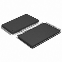
AT91SAM7SE32-AU Atmel, AT91SAM7SE32-AU Datasheet - Page 583

AT91SAM7SE32-AU
Manufacturer Part Number
AT91SAM7SE32-AU
Description
MCU ARM 32K HS FLASH 128-LQFP
Manufacturer
Atmel
Series
AT91SAMr
Specifications of AT91SAM7SE32-AU
Core Processor
ARM7
Core Size
16/32-Bit
Speed
55MHz
Connectivity
EBI/EMI, I²C, SPI, SSC, UART/USART, USB
Peripherals
Brown-out Detect/Reset, POR, PWM, WDT
Number Of I /o
88
Program Memory Size
32KB (32K x 8)
Program Memory Type
FLASH
Ram Size
8K x 8
Voltage - Supply (vcc/vdd)
1.65 V ~ 1.95 V
Data Converters
A/D 8x10b
Oscillator Type
Internal
Operating Temperature
-40°C ~ 85°C
Package / Case
128-LQFP
Controller Family/series
AT91SAM7xxxx
No. Of I/o's
88
Ram Memory Size
8KB
Cpu Speed
48MHz
No. Of Timers
3
Rohs Compliant
Yes
Processor Series
AT91SAMx
Core
ARM7TDMI
Data Bus Width
32 bit
Data Ram Size
8 KB
Interface Type
EBI, SPI, TWI, USART
Maximum Clock Frequency
55 MHz
Number Of Programmable I/os
88
Number Of Timers
3
Maximum Operating Temperature
+ 85 C
Mounting Style
SMD/SMT
3rd Party Development Tools
JTRACE-ARM-2M, KSK-AT91SAM7S-PL, MDK-ARM, RL-ARM, ULINK2
Development Tools By Supplier
AT91SAM-ICE, AT91-ISP, AT91SAM7SE-EK
Minimum Operating Temperature
- 40 C
On-chip Adc
10 bit, 8 Channel
For Use With
AT91SAM7SE-EK - EVAL BOARD FOR AT91SAM7SEAT91SAM-ICE - EMULATOR FOR AT91 ARM7/ARM9
Lead Free Status / RoHS Status
Lead free / RoHS Compliant
Eeprom Size
-
Lead Free Status / Rohs Status
Details
Available stocks
Company
Part Number
Manufacturer
Quantity
Price
Company:
Part Number:
AT91SAM7SE32-AU
Manufacturer:
ATMEL
Quantity:
624
Part Number:
AT91SAM7SE32-AU
Manufacturer:
ATMEL/爱特梅尔
Quantity:
20 000
- Current page: 583 of 655
- Download datasheet (8Mb)
Read (Set by the USB peripheral):
0 = No data packet has been received in the FIFO's Bank 1.
1 = A data packet has been received, it has been stored in FIFO's Bank 1.
When the device firmware has polled this bit or has been interrupted by this signal, it must transfer data from the FIFO to
microcontroller memory. The number of bytes received is available in RXBYTECNT field. Bank 1 FIFO values are read
through UDP_ FDRx register. Once a transfer is done, the device firmware must release Bank 1 to the USB device by
clearing RX_DATA_BK1.
• DIR: Transfer Direction (only available for control endpoints)
Read/Write
0 = Allows Data OUT transactions in the control data stage.
1 = Enables Data IN transactions in the control data stage.
Refer to Chapter 8.5.3 of the Universal Serial Bus Specification, Rev. 2.0 for more information on the control data stage.
This bit must be set before UDP_ CSRx/RXSETUP is cleared at the end of the setup stage. According to the request sent
in the setup data packet, the data stage is either a device to host (DIR = 1) or host to device (DIR = 0) data transfer. It is not
necessary to check this bit to reverse direction for the status stage.
• EPTYPE[2:0]: Endpoint Type
Read/Write
• DTGLE: Data Toggle
Read-only
0 = Identifies DATA0 packet.
1 = Identifies DATA1 packet.
Refer to Chapter 8 of the Universal Serial Bus Specification, Rev. 2.0 for more information on DATA0, DATA1 packet
definitions.
• EPEDS: Endpoint Enable Disable
Read:
0 = Endpoint disabled.
1 = Endpoint enabled.
6222B–ATARM–26-Mar-07
000
001
101
010
110
011
111
Control
Isochronous OUT
Isochronous IN
Bulk OUT
Bulk IN
Interrupt OUT
Interrupt IN
AT91SAM7SE512/256/32 Preliminary
583
Related parts for AT91SAM7SE32-AU
Image
Part Number
Description
Manufacturer
Datasheet
Request
R

Part Number:
Description:
KIT EVAL FOR ARM AT91SAM7S
Manufacturer:
Atmel
Datasheet:

Part Number:
Description:
MCU, MPU & DSP Development Tools KICKSTART KIT ATMEL AT91SAM7S
Manufacturer:
IAR Systems

Part Number:
Description:
DEV KIT FOR AVR/AVR32
Manufacturer:
Atmel
Datasheet:

Part Number:
Description:
INTERVAL AND WIPE/WASH WIPER CONTROL IC WITH DELAY
Manufacturer:
ATMEL Corporation
Datasheet:

Part Number:
Description:
Low-Voltage Voice-Switched IC for Hands-Free Operation
Manufacturer:
ATMEL Corporation
Datasheet:

Part Number:
Description:
MONOLITHIC INTEGRATED FEATUREPHONE CIRCUIT
Manufacturer:
ATMEL Corporation
Datasheet:

Part Number:
Description:
AM-FM Receiver IC U4255BM-M
Manufacturer:
ATMEL Corporation
Datasheet:

Part Number:
Description:
Monolithic Integrated Feature Phone Circuit
Manufacturer:
ATMEL Corporation
Datasheet:

Part Number:
Description:
Multistandard Video-IF and Quasi Parallel Sound Processing
Manufacturer:
ATMEL Corporation
Datasheet:

Part Number:
Description:
High-performance EE PLD
Manufacturer:
ATMEL Corporation
Datasheet:

Part Number:
Description:
8-bit Flash Microcontroller
Manufacturer:
ATMEL Corporation
Datasheet:

Part Number:
Description:
2-Wire Serial EEPROM
Manufacturer:
ATMEL Corporation
Datasheet:


