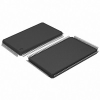
AT91SAM7SE32-AU Atmel, AT91SAM7SE32-AU Datasheet - Page 15

AT91SAM7SE32-AU
Manufacturer Part Number
AT91SAM7SE32-AU
Description
MCU ARM 32K HS FLASH 128-LQFP
Manufacturer
Atmel
Series
AT91SAMr
Specifications of AT91SAM7SE32-AU
Core Processor
ARM7
Core Size
16/32-Bit
Speed
55MHz
Connectivity
EBI/EMI, I²C, SPI, SSC, UART/USART, USB
Peripherals
Brown-out Detect/Reset, POR, PWM, WDT
Number Of I /o
88
Program Memory Size
32KB (32K x 8)
Program Memory Type
FLASH
Ram Size
8K x 8
Voltage - Supply (vcc/vdd)
1.65 V ~ 1.95 V
Data Converters
A/D 8x10b
Oscillator Type
Internal
Operating Temperature
-40°C ~ 85°C
Package / Case
128-LQFP
Controller Family/series
AT91SAM7xxxx
No. Of I/o's
88
Ram Memory Size
8KB
Cpu Speed
48MHz
No. Of Timers
3
Rohs Compliant
Yes
Processor Series
AT91SAMx
Core
ARM7TDMI
Data Bus Width
32 bit
Data Ram Size
8 KB
Interface Type
EBI, SPI, TWI, USART
Maximum Clock Frequency
55 MHz
Number Of Programmable I/os
88
Number Of Timers
3
Maximum Operating Temperature
+ 85 C
Mounting Style
SMD/SMT
3rd Party Development Tools
JTRACE-ARM-2M, KSK-AT91SAM7S-PL, MDK-ARM, RL-ARM, ULINK2
Development Tools By Supplier
AT91SAM-ICE, AT91-ISP, AT91SAM7SE-EK
Minimum Operating Temperature
- 40 C
On-chip Adc
10 bit, 8 Channel
For Use With
AT91SAM7SE-EK - EVAL BOARD FOR AT91SAM7SEAT91SAM-ICE - EMULATOR FOR AT91 ARM7/ARM9
Lead Free Status / RoHS Status
Lead free / RoHS Compliant
Eeprom Size
-
Lead Free Status / Rohs Status
Details
Available stocks
Company
Part Number
Manufacturer
Quantity
Price
Company:
Part Number:
AT91SAM7SE32-AU
Manufacturer:
ATMEL
Quantity:
624
Part Number:
AT91SAM7SE32-AU
Manufacturer:
ATMEL/爱特梅尔
Quantity:
20 000
- Current page: 15 of 655
- Download datasheet (8Mb)
6. I/O Lines Considerations
6.1
6.2
6.3
6.4
6.5
6222B–ATARM–26-Mar-07
JTAG Port Pins
Test Pin
Reset Pin
ERASE Pin
SDCK Pin
TMS, TDI and TCK are Schmitt trigger inputs. TMS, TDI and TCK do not integrate a pull-up
resistor.
TDO is an output, driven at up to VDDIO, and has no pull-up resistor.
The pin JTAGSEL is used to select the JTAG boundary scan when asserted at a high level. The
pin JTAGSEL integrates a permanent pull-down resistor of about 15 kΩ to GND, so that it can be
left unconnected for normal operations.
T h e T S T p i n i s u s e d f o r m a n u f a c t u r i n g t e s t o r f a s t p r o g r a m m i n g m o d e o f t h e
AT91SAM7SE512/256/32 when asserted high. The TST pin integrates a permanent pull-down
resistor of about 15 kΩ to GND, so that it can be left unconnected for normal operations.
To enter fast programming mode, the TST pin and the PA0 and PA1 pins should be tied high
and PA2 tied low.
Driving the TST pin at a high level while PA0 or PA1 is driven at 0 leads to unpredictable results.
The NRST pin is bidirectional. It is handled by the on-chip reset controller and can be driven low
to provide a reset signal to the external components or asserted low externally to reset the
microcontroller. There is no constraint on the length of the reset pulse, and the reset controller
can guarantee a minimum pulse length. This allows connection of a simple push-button on the
NRST pin as system user reset, and the use of the NRST signal to reset all the components of
the system.
An external power-on reset can drive this pin during the start-up instead of using the internal
power-on reset circuit.
The NRST pin integrates a permanent pull-up of about 100 kΩ resistor to VDDIO.
This pin has Schmitt trigger input.
The ERASE pin is used to re-initialize the Flash content and some of its NVM bits. It integrates a
permanent pull-down resistor of about 15 kΩ to GND, so that it can be left unconnected for nor-
mal operations.
This pin is debounced by the RC oscillator to improve the glitch tolerance. When the pin is tied to
high during less than 100 ms, ERASE pin is not taken into account. The pin must be tied high
during more than 220 ms to perform the re-initialization of the Flash.
The SDCK pin is dedicated to the SDRAM Clock and is an output-only without pull-up. Maximum
Output Frequency of this pad is 48 MHz at 3.0V and 25 MHz at 1.65V with a maximum load of
30 pF.
AT91SAM7SE512/256/32 Preliminary
15
Related parts for AT91SAM7SE32-AU
Image
Part Number
Description
Manufacturer
Datasheet
Request
R

Part Number:
Description:
KIT EVAL FOR ARM AT91SAM7S
Manufacturer:
Atmel
Datasheet:

Part Number:
Description:
MCU, MPU & DSP Development Tools KICKSTART KIT ATMEL AT91SAM7S
Manufacturer:
IAR Systems

Part Number:
Description:
DEV KIT FOR AVR/AVR32
Manufacturer:
Atmel
Datasheet:

Part Number:
Description:
INTERVAL AND WIPE/WASH WIPER CONTROL IC WITH DELAY
Manufacturer:
ATMEL Corporation
Datasheet:

Part Number:
Description:
Low-Voltage Voice-Switched IC for Hands-Free Operation
Manufacturer:
ATMEL Corporation
Datasheet:

Part Number:
Description:
MONOLITHIC INTEGRATED FEATUREPHONE CIRCUIT
Manufacturer:
ATMEL Corporation
Datasheet:

Part Number:
Description:
AM-FM Receiver IC U4255BM-M
Manufacturer:
ATMEL Corporation
Datasheet:

Part Number:
Description:
Monolithic Integrated Feature Phone Circuit
Manufacturer:
ATMEL Corporation
Datasheet:

Part Number:
Description:
Multistandard Video-IF and Quasi Parallel Sound Processing
Manufacturer:
ATMEL Corporation
Datasheet:

Part Number:
Description:
High-performance EE PLD
Manufacturer:
ATMEL Corporation
Datasheet:

Part Number:
Description:
8-bit Flash Microcontroller
Manufacturer:
ATMEL Corporation
Datasheet:

Part Number:
Description:
2-Wire Serial EEPROM
Manufacturer:
ATMEL Corporation
Datasheet:


