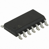
ATTINY44A-SSN Atmel, ATTINY44A-SSN Datasheet - Page 89

ATTINY44A-SSN
Manufacturer Part Number
ATTINY44A-SSN
Description
IC MCU AVR 4KB FLASH 20MHZ 14SOI
Manufacturer
Atmel
Series
AVR® ATtinyr
Specifications of ATTINY44A-SSN
Core Processor
AVR
Core Size
8-Bit
Speed
20MHz
Connectivity
USI
Peripherals
Brown-out Detect/Reset, POR, PWM, Temp Sensor, WDT
Number Of I /o
12
Program Memory Size
4KB (2K x 16)
Program Memory Type
FLASH
Eeprom Size
256 x 8
Ram Size
256 x 8
Voltage - Supply (vcc/vdd)
1.8 V ~ 5.5 V
Data Converters
A/D 8x10b
Oscillator Type
Internal
Operating Temperature
-40°C ~ 85°C
Package / Case
14-SOIC (3.9mm Width), 14-SOL
Processor Series
ATTINY4x
Core
AVR8
Data Bus Width
8 bit
Data Ram Size
256 B
Interface Type
SPI
Maximum Clock Frequency
20 MHz
Number Of Programmable I/os
12
Operating Supply Voltage
1.8 V to 5.5 V
Maximum Operating Temperature
+ 85 C
Mounting Style
SMD/SMT
3rd Party Development Tools
EWAVR, EWAVR-BL
Development Tools By Supplier
ATAVRDRAGON, ATSTK500, ATSTK600, ATAVRISP2, ATAVRONEKIT
Minimum Operating Temperature
- 40 C
Lead Free Status / RoHS Status
Lead free / RoHS Compliant
- Current page: 89 of 286
- Download datasheet (10Mb)
12.5.1
8183C–AVR–03/11
Input Capture Trigger Source
Figure 12-3.
When a change of the logic level (an event) occurs on the Input Capture pin (ICP1), alternatively
on the Analog Comparator output (ACO), and this change confirms to the setting of the edge
detector, a capture will be triggered. When a capture is triggered, the 16-bit value of the counter
(TCNT1) is written to the Input Capture Register (ICR1). The Input Capture Flag (ICF1) is set at
the same system clock as the TCNT1 value is copied into ICR1 Register. If enabled (ICIE1 = 1),
the Input Capture Flag generates an Input Capture interrupt. The ICF1 flag is automatically
cleared when the interrupt is executed. Alternatively the ICF1 flag can be cleared by software by
writing a logical one to its I/O bit location.
Reading the 16-bit value in the Input Capture Register (ICR1) is done by first reading the low
byte (ICR1L) and then the high byte (ICR1H). When the low byte is read the high byte is copied
into the high byte temporary register (TEMP). When the CPU reads the ICR1H I/O location it will
access the TEMP Register.
The ICR1 Register can only be written when using a Waveform Generation mode that utilizes
the ICR1 Register for defining the counter’s TOP value. In these cases the Waveform Genera-
tion mode (WGM1[3:0]) bits must be set before the TOP value can be written to the ICR1
Register. When writing the ICR1 Register the high byte must be written to the ICR1H I/O location
before the low byte is written to ICR1L.
For more information on how to access the 16-bit registers refer to
on page
The main trigger source for the Input Capture unit is the Input Capture pin (ICP1).
Timer/Counter1 can alternatively use the Analog Comparator output as trigger source for the
Input Capture unit. The Analog Comparator is selected as trigger source by setting the Analog
Comparator Input Capture (ACIC) bit in the Analog Comparator Control and Status Register
ICPn
WRITE
103.
ICRnH (8-bit)
TEMP (8-bit)
Comparator
Analog
Input Capture Unit Block Diagram
ICRn (16-bit Register)
ACO*
ICRnL (8-bit)
ACIC*
DATA BUS
Canceler
Noise
ICNC
(8-bit)
TCNTnH (8-bit)
ATtiny24A/44A/84A
TCNTn (16-bit Counter)
Detector
ICES
Edge
“Accessing 16-bit Registers”
TCNTnL (8-bit)
ICFn (Int.Req.)
89
Related parts for ATTINY44A-SSN
Image
Part Number
Description
Manufacturer
Datasheet
Request
R

Part Number:
Description:
Manufacturer:
Atmel Corporation
Datasheet:

Part Number:
Description:
Manufacturer:
Atmel Corporation
Datasheet:

Part Number:
Description:
MCU AVR 4K FLASH 15MHZ 20-QFN
Manufacturer:
Atmel
Datasheet:

Part Number:
Description:
IC MCU AVR 4K FLASH 20MHZ 20-QFN
Manufacturer:
Atmel
Datasheet:

Part Number:
Description:
IC MCU AVR 4K FLASH 20MHZ 14SOIC
Manufacturer:
Atmel
Datasheet:

Part Number:
Description:
MCU AVR 4KB FLASH 20MHZ 14SOIC
Manufacturer:
Atmel
Datasheet:

Part Number:
Description:
MCU AVR 4KB FLASH 20MHZ 20QFN
Manufacturer:
Atmel
Datasheet:

Part Number:
Description:
IC MCU AVR 4K FLASH 15MHZ 14SOIC
Manufacturer:
Atmel
Datasheet:

Part Number:
Description:
IC MCU AVR 4K FLASH 20MHZ 14-DIP
Manufacturer:
Atmel
Datasheet:

Part Number:
Description:
Manufacturer:
Atmel Corporation
Datasheet:

Part Number:
Description:
Microcontrollers (MCU) 512B FL 32B SRAM TIMER ATTINY4 12MHz
Manufacturer:
Atmel

Part Number:
Description:
IC MCU AVR 512B FLASH SOT-23-6
Manufacturer:
Atmel
Datasheet:

Part Number:
Description:
IC MCU AVR 512B FLASH SOT-23-6
Manufacturer:
Atmel
Datasheet:


