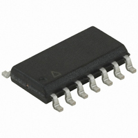
ATTINY44A-SSN Atmel, ATTINY44A-SSN Datasheet - Page 121

ATTINY44A-SSN
Manufacturer Part Number
ATTINY44A-SSN
Description
IC MCU AVR 4KB FLASH 20MHZ 14SOI
Manufacturer
Atmel
Series
AVR® ATtinyr
Specifications of ATTINY44A-SSN
Core Processor
AVR
Core Size
8-Bit
Speed
20MHz
Connectivity
USI
Peripherals
Brown-out Detect/Reset, POR, PWM, Temp Sensor, WDT
Number Of I /o
12
Program Memory Size
4KB (2K x 16)
Program Memory Type
FLASH
Eeprom Size
256 x 8
Ram Size
256 x 8
Voltage - Supply (vcc/vdd)
1.8 V ~ 5.5 V
Data Converters
A/D 8x10b
Oscillator Type
Internal
Operating Temperature
-40°C ~ 85°C
Package / Case
14-SOIC (3.9mm Width), 14-SOL
Processor Series
ATTINY4x
Core
AVR8
Data Bus Width
8 bit
Data Ram Size
256 B
Interface Type
SPI
Maximum Clock Frequency
20 MHz
Number Of Programmable I/os
12
Operating Supply Voltage
1.8 V to 5.5 V
Maximum Operating Temperature
+ 85 C
Mounting Style
SMD/SMT
3rd Party Development Tools
EWAVR, EWAVR-BL
Development Tools By Supplier
ATAVRDRAGON, ATSTK500, ATSTK600, ATAVRISP2, ATAVRONEKIT
Minimum Operating Temperature
- 40 C
Lead Free Status / RoHS Status
Lead free / RoHS Compliant
- Current page: 121 of 286
- Download datasheet (10Mb)
8183C–AVR–03/11
Figure 14-4.
The data direction is not given by the physical layer. A protocol, like the one used by the TWI-
bus, must be implemented to control the data flow.
Figure 14-5.
Referring to the timing diagram
SDA
SCL
1. The start condition is generated by the master by forcing the SDA low line while keep-
2. In addition, the start detector will hold the SCL line low after the master has forced a
3. The master set the first bit to be transferred and releases the SCL line (C). The slave
ing the SCL line high (A). SDA can be forced low either by writing a zero to bit 7 of the
USI Data Register, or by setting the corresponding bit in the PORTA register to zero.
Note that the Data Direction Register bit must be set to one for the output to be
enabled. The start detector logic of the slave device (see
detects the start condition and sets the USISIF Flag. The flag can generate an interrupt
if necessary.
negative edge on this line (B). This allows the slave to wake up from sleep or complete
other tasks before setting up the USI Data Register to receive the address. This is done
by clearing the start condition flag and resetting the counter.
samples the data and shifts it into the USI Data Register at the positive edge of the SCL
clock.
SLAVE
MASTER
A B
S
Bit7
Bit7
Two-wire Mode Operation, Simplified Diagram
Two-wire Mode, Typical Timing Diagram
Bit6
Bit6
C
ADDRESS
1 - 7
Bit5
Bit5
Bit4
Bit4
Bit3
Bit3
R/W
(Figure
8
D
Bit2
Bit2
Bit1
Bit1
14-5), a bus transfer involves the following steps:
ACK
9
Bit0
Bit0
E
DATA
1 - 8
Two-wire Clock
Control Unit
ATtiny24A/44A/84A
ACK
9
PORTxn
Figure 14-6 on page
HOLD
SCL
DATA
1 - 8
SDA
SCL
SDA
SCL
ACK
9
VCC
122)
P
F
121
Related parts for ATTINY44A-SSN
Image
Part Number
Description
Manufacturer
Datasheet
Request
R

Part Number:
Description:
Manufacturer:
Atmel Corporation
Datasheet:

Part Number:
Description:
Manufacturer:
Atmel Corporation
Datasheet:

Part Number:
Description:
MCU AVR 4K FLASH 15MHZ 20-QFN
Manufacturer:
Atmel
Datasheet:

Part Number:
Description:
IC MCU AVR 4K FLASH 20MHZ 20-QFN
Manufacturer:
Atmel
Datasheet:

Part Number:
Description:
IC MCU AVR 4K FLASH 20MHZ 14SOIC
Manufacturer:
Atmel
Datasheet:

Part Number:
Description:
MCU AVR 4KB FLASH 20MHZ 14SOIC
Manufacturer:
Atmel
Datasheet:

Part Number:
Description:
MCU AVR 4KB FLASH 20MHZ 20QFN
Manufacturer:
Atmel
Datasheet:

Part Number:
Description:
IC MCU AVR 4K FLASH 15MHZ 14SOIC
Manufacturer:
Atmel
Datasheet:

Part Number:
Description:
IC MCU AVR 4K FLASH 20MHZ 14-DIP
Manufacturer:
Atmel
Datasheet:

Part Number:
Description:
Manufacturer:
Atmel Corporation
Datasheet:

Part Number:
Description:
Microcontrollers (MCU) 512B FL 32B SRAM TIMER ATTINY4 12MHz
Manufacturer:
Atmel

Part Number:
Description:
IC MCU AVR 512B FLASH SOT-23-6
Manufacturer:
Atmel
Datasheet:

Part Number:
Description:
IC MCU AVR 512B FLASH SOT-23-6
Manufacturer:
Atmel
Datasheet:


