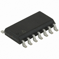
ATTINY44A-SSN Atmel, ATTINY44A-SSN Datasheet - Page 127

ATTINY44A-SSN
Manufacturer Part Number
ATTINY44A-SSN
Description
IC MCU AVR 4KB FLASH 20MHZ 14SOI
Manufacturer
Atmel
Series
AVR® ATtinyr
Specifications of ATTINY44A-SSN
Core Processor
AVR
Core Size
8-Bit
Speed
20MHz
Connectivity
USI
Peripherals
Brown-out Detect/Reset, POR, PWM, Temp Sensor, WDT
Number Of I /o
12
Program Memory Size
4KB (2K x 16)
Program Memory Type
FLASH
Eeprom Size
256 x 8
Ram Size
256 x 8
Voltage - Supply (vcc/vdd)
1.8 V ~ 5.5 V
Data Converters
A/D 8x10b
Oscillator Type
Internal
Operating Temperature
-40°C ~ 85°C
Package / Case
14-SOIC (3.9mm Width), 14-SOL
Processor Series
ATTINY4x
Core
AVR8
Data Bus Width
8 bit
Data Ram Size
256 B
Interface Type
SPI
Maximum Clock Frequency
20 MHz
Number Of Programmable I/os
12
Operating Supply Voltage
1.8 V to 5.5 V
Maximum Operating Temperature
+ 85 C
Mounting Style
SMD/SMT
3rd Party Development Tools
EWAVR, EWAVR-BL
Development Tools By Supplier
ATAVRDRAGON, ATSTK500, ATSTK600, ATAVRISP2, ATAVRONEKIT
Minimum Operating Temperature
- 40 C
Lead Free Status / RoHS Status
Lead free / RoHS Compliant
- Current page: 127 of 286
- Download datasheet (10Mb)
14.5.4
8183C–AVR–03/11
USIBR – USI Buffer Register
Note that even when no wire mode is selected (USIWM[1:0] = 0) both the external data input
(DI/SDA) and the external clock input (USCK/SCL) can still be used by the USI Data Register.
The output pin (DO or SDA, depending on the wire mode) is connected via the output latch to
the most significant bit (bit 7) of the USI Data Register. The output latch ensures that data input
is sampled and data output is changed on opposite clock edges. The latch is open (transparent)
during the first half of a serial clock cycle when an external clock source is selected (USICS1 =
1) and constantly open when an internal clock source is used (USICS1 = 0). The output will be
changed immediately when a new MSB is written as long as the latch is open.
Note that the Data Direction Register bit corresponding to the output pin must be set to one in
order to enable data output from the USI Data Register.
Instead of reading data from the USI Data Register the USI Buffer Register can be used. This
makes controlling the USI less time critical and gives the CPU more time to handle other pro-
gram tasks. USI flags as set similarly as when reading the USIDR register.
The content of the USI Data Register is loaded to the USI Buffer Register when the transfer has
been completed.
Bit
0x10 (0x30)
Read/Write
Initial Value
MSB
R
7
0
R
6
0
R
5
0
R
4
0
R
3
0
ATtiny24A/44A/84A
R
2
0
R
1
0
LSB
R
0
0
USIBR
127
Related parts for ATTINY44A-SSN
Image
Part Number
Description
Manufacturer
Datasheet
Request
R

Part Number:
Description:
Manufacturer:
Atmel Corporation
Datasheet:

Part Number:
Description:
Manufacturer:
Atmel Corporation
Datasheet:

Part Number:
Description:
MCU AVR 4K FLASH 15MHZ 20-QFN
Manufacturer:
Atmel
Datasheet:

Part Number:
Description:
IC MCU AVR 4K FLASH 20MHZ 20-QFN
Manufacturer:
Atmel
Datasheet:

Part Number:
Description:
IC MCU AVR 4K FLASH 20MHZ 14SOIC
Manufacturer:
Atmel
Datasheet:

Part Number:
Description:
MCU AVR 4KB FLASH 20MHZ 14SOIC
Manufacturer:
Atmel
Datasheet:

Part Number:
Description:
MCU AVR 4KB FLASH 20MHZ 20QFN
Manufacturer:
Atmel
Datasheet:

Part Number:
Description:
IC MCU AVR 4K FLASH 15MHZ 14SOIC
Manufacturer:
Atmel
Datasheet:

Part Number:
Description:
IC MCU AVR 4K FLASH 20MHZ 14-DIP
Manufacturer:
Atmel
Datasheet:

Part Number:
Description:
Manufacturer:
Atmel Corporation
Datasheet:

Part Number:
Description:
Microcontrollers (MCU) 512B FL 32B SRAM TIMER ATTINY4 12MHz
Manufacturer:
Atmel

Part Number:
Description:
IC MCU AVR 512B FLASH SOT-23-6
Manufacturer:
Atmel
Datasheet:

Part Number:
Description:
IC MCU AVR 512B FLASH SOT-23-6
Manufacturer:
Atmel
Datasheet:


