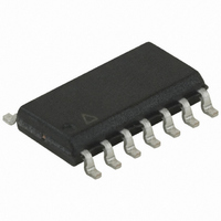
ATTINY44A-SSN Atmel, ATTINY44A-SSN Datasheet - Page 116

ATTINY44A-SSN
Manufacturer Part Number
ATTINY44A-SSN
Description
IC MCU AVR 4KB FLASH 20MHZ 14SOI
Manufacturer
Atmel
Series
AVR® ATtinyr
Specifications of ATTINY44A-SSN
Core Processor
AVR
Core Size
8-Bit
Speed
20MHz
Connectivity
USI
Peripherals
Brown-out Detect/Reset, POR, PWM, Temp Sensor, WDT
Number Of I /o
12
Program Memory Size
4KB (2K x 16)
Program Memory Type
FLASH
Eeprom Size
256 x 8
Ram Size
256 x 8
Voltage - Supply (vcc/vdd)
1.8 V ~ 5.5 V
Data Converters
A/D 8x10b
Oscillator Type
Internal
Operating Temperature
-40°C ~ 85°C
Package / Case
14-SOIC (3.9mm Width), 14-SOL
Processor Series
ATTINY4x
Core
AVR8
Data Bus Width
8 bit
Data Ram Size
256 B
Interface Type
SPI
Maximum Clock Frequency
20 MHz
Number Of Programmable I/os
12
Operating Supply Voltage
1.8 V to 5.5 V
Maximum Operating Temperature
+ 85 C
Mounting Style
SMD/SMT
3rd Party Development Tools
EWAVR, EWAVR-BL
Development Tools By Supplier
ATAVRDRAGON, ATSTK500, ATSTK600, ATAVRISP2, ATAVRONEKIT
Minimum Operating Temperature
- 40 C
Lead Free Status / RoHS Status
Lead free / RoHS Compliant
- Current page: 116 of 286
- Download datasheet (10Mb)
14. USI – Universal Serial Interface
14.1
14.2
116
Features
Overview
ATtiny24A/44A/84A
•
•
•
•
•
•
The Universal Serial Interface (USI), provides the basic hardware resources needed for serial
communication. Combined with a minimum of control software, the USI allows significantly
higher transfer rates and uses less code space than solutions based on software only. Interrupts
are included to minimize the processor load.
A simplified block diagram of the USI is shown in
refer to
are listed in the
Figure 14-1.
The 8-bit USI Data Register (USIDR) contains the incoming and outgoing data. It is directly
accessible via the data bus but a copy of the contents is also placed in the USI Buffer Register
(USIBR) where it can be retrieved later. If reading the USI Data Register directly, the register
must be read as quickly as possible to ensure that no data is lost.
The most significant bit of the USI Data Register is connected to one of two output pins (depend-
ing on the mode configuration, see
latch between the output of the USI Data Register and the output pin, which delays the change
of data output to the opposite clock edge of the data input sampling. The serial input is always
sampled from the Data Input (DI) pin independent of the configuration.
Two-wire Synchronous Data Transfer (Master or Slave)
Three-wire Synchronous Data Transfer (Master or Slave)
Data Received Interrupt
Wakeup from Idle Mode
In Two-wire Mode: Wake-up from All Sleep Modes, Including Power-down Mode
Two-wire Start Condition Detector with Interrupt Capability
“Pinout of ATtiny24A/44A/84A” on page
“Register Descriptions” on page
USIDR
USIBR
USISR
USICR
Universal Serial Interface, Block Diagram
2
4-bit Counter
“Analog Comparator” on page
3
2
1
0
3
2
1
0
D Q
LE
[1]
2. Device-specific I/O Register and bit locations
123.
TIM0 COMP
Figure 14-1
0
1
Two-wire Clock
Control Unit
For actual placement of I/O pins
128). There is a transparent
CLOCK
HOLD
DO
DI/SDA
USCK/SCL
8183C–AVR–03/11
(Output only)
(Input/Open Drain)
(Input/Open Drain)
Related parts for ATTINY44A-SSN
Image
Part Number
Description
Manufacturer
Datasheet
Request
R

Part Number:
Description:
Manufacturer:
Atmel Corporation
Datasheet:

Part Number:
Description:
Manufacturer:
Atmel Corporation
Datasheet:

Part Number:
Description:
MCU AVR 4K FLASH 15MHZ 20-QFN
Manufacturer:
Atmel
Datasheet:

Part Number:
Description:
IC MCU AVR 4K FLASH 20MHZ 20-QFN
Manufacturer:
Atmel
Datasheet:

Part Number:
Description:
IC MCU AVR 4K FLASH 20MHZ 14SOIC
Manufacturer:
Atmel
Datasheet:

Part Number:
Description:
MCU AVR 4KB FLASH 20MHZ 14SOIC
Manufacturer:
Atmel
Datasheet:

Part Number:
Description:
MCU AVR 4KB FLASH 20MHZ 20QFN
Manufacturer:
Atmel
Datasheet:

Part Number:
Description:
IC MCU AVR 4K FLASH 15MHZ 14SOIC
Manufacturer:
Atmel
Datasheet:

Part Number:
Description:
IC MCU AVR 4K FLASH 20MHZ 14-DIP
Manufacturer:
Atmel
Datasheet:

Part Number:
Description:
Manufacturer:
Atmel Corporation
Datasheet:

Part Number:
Description:
Microcontrollers (MCU) 512B FL 32B SRAM TIMER ATTINY4 12MHz
Manufacturer:
Atmel

Part Number:
Description:
IC MCU AVR 512B FLASH SOT-23-6
Manufacturer:
Atmel
Datasheet:

Part Number:
Description:
IC MCU AVR 512B FLASH SOT-23-6
Manufacturer:
Atmel
Datasheet:


