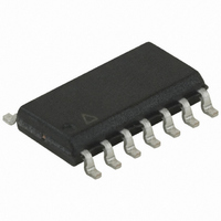
ATTINY44A-SSN Atmel, ATTINY44A-SSN Datasheet - Page 58

ATTINY44A-SSN
Manufacturer Part Number
ATTINY44A-SSN
Description
IC MCU AVR 4KB FLASH 20MHZ 14SOI
Manufacturer
Atmel
Series
AVR® ATtinyr
Specifications of ATTINY44A-SSN
Core Processor
AVR
Core Size
8-Bit
Speed
20MHz
Connectivity
USI
Peripherals
Brown-out Detect/Reset, POR, PWM, Temp Sensor, WDT
Number Of I /o
12
Program Memory Size
4KB (2K x 16)
Program Memory Type
FLASH
Eeprom Size
256 x 8
Ram Size
256 x 8
Voltage - Supply (vcc/vdd)
1.8 V ~ 5.5 V
Data Converters
A/D 8x10b
Oscillator Type
Internal
Operating Temperature
-40°C ~ 85°C
Package / Case
14-SOIC (3.9mm Width), 14-SOL
Processor Series
ATTINY4x
Core
AVR8
Data Bus Width
8 bit
Data Ram Size
256 B
Interface Type
SPI
Maximum Clock Frequency
20 MHz
Number Of Programmable I/os
12
Operating Supply Voltage
1.8 V to 5.5 V
Maximum Operating Temperature
+ 85 C
Mounting Style
SMD/SMT
3rd Party Development Tools
EWAVR, EWAVR-BL
Development Tools By Supplier
ATAVRDRAGON, ATSTK500, ATSTK600, ATAVRISP2, ATAVRONEKIT
Minimum Operating Temperature
- 40 C
Lead Free Status / RoHS Status
Lead free / RoHS Compliant
- Current page: 58 of 286
- Download datasheet (10Mb)
10.2
58
Alternate Port Functions
ATtiny24A/44A/84A
Most port pins have alternate functions in addition to being general digital I/Os. In
below is shown how the port pin control signals from the simplified
be overridden by alternate functions.
Figure 10-5.
Note:
The illustration in the figure above serves as a generic description applicable to all port pins in
the AVR microcontroller family. Some overriding signals may not be present in all port pins.
PUOExn:
PUOVxn:
DDOExn:
DDOVxn:
PVOExn:
PVOVxn:
DIEOExn: Pxn DIGITAL INPUT-ENABLE OVERRIDE ENABLE
DIEOVxn: Pxn DIGITAL INPUT-ENABLE OVERRIDE VALUE
SLEEP:
PTOExn:
Pxn
1. WRx, WPx, WDx, RRx, RPx, and RDx are common to all pins within the same port. clk
Pxn, PORT TOGGLE OVERRIDE ENABLE
Pxn PULL-UP OVERRIDE ENABLE
Pxn PULL-UP OVERRIDE VALUE
Pxn DATA DIRECTION OVERRIDE ENABLE
Pxn DATA DIRECTION OVERRIDE VALUE
Pxn PORT VALUE OVERRIDE ENABLE
Pxn PORT VALUE OVERRIDE VALUE
SLEEP CONTROL
SLEEP, and PUD are common to all ports. All other signals are unique for each pin.
Alternate Port Functions
1
0
1
0
1
0
1
0
PUOExn
PUOVxn
DIEOExn
DDOExn
DDOVxn
PVOExn
PVOVxn
DIEOVxn
SLEEP
(1)
SYNCHRONIZER
D
L
SET
CLR
Q
Q
PUD:
WDx:
RDx:
RRx:
WRx:
RPx:
WPx:
clk
DIxn:
AIOxn:
D
PINxn
CLR
I/O
Q
Q
:
RESET
PORTxn
Q
Q
CLR
D
RESET
Q
Q
DDxn
CLR
WRITE DDRx
WRITE PORTx
PULLUP DISABLE
READ DDRx
READ PORTx REGISTER
READ PORTx PIN
WRITE PINx
I/O CLOCK
DIGITAL INPUT PIN n ON PORTx
ANALOG INPUT/OUTPUT PIN n ON PORTx
D
1
0
RRx
Figure 10-2 on page 54
clk
PUD
WDx
RDx
DIxn
AIOxn
RPx
I/O
WRx
PTOExn
8183C–AVR–03/11
WPx
Figure 10-5
I/O
,
can
Related parts for ATTINY44A-SSN
Image
Part Number
Description
Manufacturer
Datasheet
Request
R

Part Number:
Description:
Manufacturer:
Atmel Corporation
Datasheet:

Part Number:
Description:
Manufacturer:
Atmel Corporation
Datasheet:

Part Number:
Description:
MCU AVR 4K FLASH 15MHZ 20-QFN
Manufacturer:
Atmel
Datasheet:

Part Number:
Description:
IC MCU AVR 4K FLASH 20MHZ 20-QFN
Manufacturer:
Atmel
Datasheet:

Part Number:
Description:
IC MCU AVR 4K FLASH 20MHZ 14SOIC
Manufacturer:
Atmel
Datasheet:

Part Number:
Description:
MCU AVR 4KB FLASH 20MHZ 14SOIC
Manufacturer:
Atmel
Datasheet:

Part Number:
Description:
MCU AVR 4KB FLASH 20MHZ 20QFN
Manufacturer:
Atmel
Datasheet:

Part Number:
Description:
IC MCU AVR 4K FLASH 15MHZ 14SOIC
Manufacturer:
Atmel
Datasheet:

Part Number:
Description:
IC MCU AVR 4K FLASH 20MHZ 14-DIP
Manufacturer:
Atmel
Datasheet:

Part Number:
Description:
Manufacturer:
Atmel Corporation
Datasheet:

Part Number:
Description:
Microcontrollers (MCU) 512B FL 32B SRAM TIMER ATTINY4 12MHz
Manufacturer:
Atmel

Part Number:
Description:
IC MCU AVR 512B FLASH SOT-23-6
Manufacturer:
Atmel
Datasheet:

Part Number:
Description:
IC MCU AVR 512B FLASH SOT-23-6
Manufacturer:
Atmel
Datasheet:


