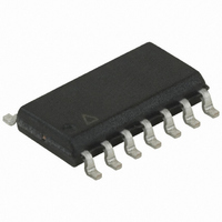
ATTINY44A-SSN Atmel, ATTINY44A-SSN Datasheet - Page 143

ATTINY44A-SSN
Manufacturer Part Number
ATTINY44A-SSN
Description
IC MCU AVR 4KB FLASH 20MHZ 14SOI
Manufacturer
Atmel
Series
AVR® ATtinyr
Specifications of ATTINY44A-SSN
Core Processor
AVR
Core Size
8-Bit
Speed
20MHz
Connectivity
USI
Peripherals
Brown-out Detect/Reset, POR, PWM, Temp Sensor, WDT
Number Of I /o
12
Program Memory Size
4KB (2K x 16)
Program Memory Type
FLASH
Eeprom Size
256 x 8
Ram Size
256 x 8
Voltage - Supply (vcc/vdd)
1.8 V ~ 5.5 V
Data Converters
A/D 8x10b
Oscillator Type
Internal
Operating Temperature
-40°C ~ 85°C
Package / Case
14-SOIC (3.9mm Width), 14-SOL
Processor Series
ATTINY4x
Core
AVR8
Data Bus Width
8 bit
Data Ram Size
256 B
Interface Type
SPI
Maximum Clock Frequency
20 MHz
Number Of Programmable I/os
12
Operating Supply Voltage
1.8 V to 5.5 V
Maximum Operating Temperature
+ 85 C
Mounting Style
SMD/SMT
3rd Party Development Tools
EWAVR, EWAVR-BL
Development Tools By Supplier
ATAVRDRAGON, ATSTK500, ATSTK600, ATAVRISP2, ATAVRONEKIT
Minimum Operating Temperature
- 40 C
Lead Free Status / RoHS Status
Lead free / RoHS Compliant
- Current page: 143 of 286
- Download datasheet (10Mb)
16.11.3
16.12 Temperature Measurement
8183C–AVR–03/11
Bipolar Differential Conversion
If differential channels and a bipolar input mode are used, the result is
where V
and V
0x200 (-512d) through 0x1FF (+511d). The GAIN is either 1x or 20x. Note that if the user wants
to perform a quick polarity check of the result, it is sufficient to read the MSB of the result (ADC9
in ADCH). If the bit is one, the result is negative, and if this bit is zero, the result is positive.
As default the ADC converter operates in the unipolar input mode, but the bipolar input mode
can be selected by writting the BIN bit in the ADCSRB to one. In the bipolar input mode two-
sided voltage differences are allowed and thus the voltage on the negative input pin can also be
larger than the voltage on the positive input pin.
The temperature measurement is based on an on-chip temperature sensor that is coupled to a
single ended ADC8 channel. Selecting the ADC8 channel by writing the MUX[5:0] bits in
ADMUX register to “100010” enables the temperature sensor. The internal 1.1V reference must
also be selected for the ADC reference source in the temperature sensor measurement. When
the temperature sensor is enabled, the ADC converter can be used in single conversion mode to
measure the voltage over the temperature sensor.
The measured voltage has a linear relationship to the temperature as described in
The sensitivity is approximately 1 LSB / °C and the accuracy depends on the method of user cal-
ibration. Typically, the measurement accuracy after a single temperature calibration is ±
assuming calibration at room temperature. Better accuracies are achieved by using two
temperature points for calibration.
Table 16-2.
The values described in
temperature sensor output voltage varies from one chip to another. To be capable of achieving
more accurate results the temperature measurement can be calibrated in the application soft-
ware. The sofware calibration can be done using the formula:
where ADCH and ADCL are the ADC data registers, k is the fixed slope coefficient and T
temperature sensor offset. Typically, k is very close to 1.0 and in single-point calibration the
coefficient may be omitted. Where higher accuracy is required the slope coefficient should be
evaluated based on measurements at two temperatures.
Temperature
ADC
T = k * [(ADCH << 8) | ADCL] + T
REF
POS
the selected voltage reference. The result is presented in two’s complement form, from
is the voltage on the positive input pin, V
Temperature vs. Sensor Output Voltage (Typical Case)
Table 16-2
ADC
230 LSB
-40
=
°
C
(
---------------------------------------------------- - GAIN
are typical values. However, due to process variation the
V
POS
OS
–
V
V
REF
NEG
) 512
⋅
NEG
300 LSB
+25
⋅
the voltage on the negative input pin,
ATtiny24A/44A/84A
°
C
370 LSB
+85
Table 16-2
°
C
OS
10
is the
143
°C,
Related parts for ATTINY44A-SSN
Image
Part Number
Description
Manufacturer
Datasheet
Request
R

Part Number:
Description:
Manufacturer:
Atmel Corporation
Datasheet:

Part Number:
Description:
Manufacturer:
Atmel Corporation
Datasheet:

Part Number:
Description:
MCU AVR 4K FLASH 15MHZ 20-QFN
Manufacturer:
Atmel
Datasheet:

Part Number:
Description:
IC MCU AVR 4K FLASH 20MHZ 20-QFN
Manufacturer:
Atmel
Datasheet:

Part Number:
Description:
IC MCU AVR 4K FLASH 20MHZ 14SOIC
Manufacturer:
Atmel
Datasheet:

Part Number:
Description:
MCU AVR 4KB FLASH 20MHZ 14SOIC
Manufacturer:
Atmel
Datasheet:

Part Number:
Description:
MCU AVR 4KB FLASH 20MHZ 20QFN
Manufacturer:
Atmel
Datasheet:

Part Number:
Description:
IC MCU AVR 4K FLASH 15MHZ 14SOIC
Manufacturer:
Atmel
Datasheet:

Part Number:
Description:
IC MCU AVR 4K FLASH 20MHZ 14-DIP
Manufacturer:
Atmel
Datasheet:

Part Number:
Description:
Manufacturer:
Atmel Corporation
Datasheet:

Part Number:
Description:
Microcontrollers (MCU) 512B FL 32B SRAM TIMER ATTINY4 12MHz
Manufacturer:
Atmel

Part Number:
Description:
IC MCU AVR 512B FLASH SOT-23-6
Manufacturer:
Atmel
Datasheet:

Part Number:
Description:
IC MCU AVR 512B FLASH SOT-23-6
Manufacturer:
Atmel
Datasheet:


