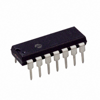
PIC16F688-E/P Microchip Technology, PIC16F688-E/P Datasheet - Page 445

PIC16F688-E/P
Manufacturer Part Number
PIC16F688-E/P
Description
IC MCU PIC FLASH 4KX14 14DIP
Manufacturer
Microchip Technology
Series
PIC® 16Fr
Datasheets
1.PIC16F616T-ISL.pdf
(8 pages)
2.PIC16F688T-ISL.pdf
(204 pages)
3.PIC16F688T-ISL.pdf
(6 pages)
4.PIC16F688T-ISL.pdf
(4 pages)
5.PIC16F688T-ISL.pdf
(688 pages)
6.PIC16F688-EP.pdf
(174 pages)
Specifications of PIC16F688-E/P
Program Memory Type
FLASH
Program Memory Size
7KB (4K x 14)
Package / Case
14-DIP (0.300", 7.62mm)
Core Processor
PIC
Core Size
8-Bit
Speed
20MHz
Connectivity
UART/USART
Peripherals
Brown-out Detect/Reset, POR, WDT
Number Of I /o
12
Eeprom Size
256 x 8
Ram Size
256 x 8
Voltage - Supply (vcc/vdd)
2 V ~ 5.5 V
Data Converters
A/D 8x10b
Oscillator Type
Internal
Operating Temperature
-40°C ~ 125°C
Processor Series
PIC16F
Core
PIC
Data Bus Width
8 bit
Data Ram Size
256 B
Interface Type
SCI/USART
Maximum Clock Frequency
20 MHz
Number Of Programmable I/os
12
Number Of Timers
2
Operating Supply Voltage
2 V to 5.5 V
Maximum Operating Temperature
+ 125 C
Mounting Style
Through Hole
3rd Party Development Tools
52715-96, 52716-328, 52717-734
Development Tools By Supplier
PG164130, DV164035, DV244005, DV164005, PG164120, ICE2000, DM163014, DM164120-4
Minimum Operating Temperature
- 40 C
On-chip Adc
8-ch x 10-bit
Lead Free Status / RoHS Status
Lead free / RoHS Compliant
For Use With
AC162066 - HEADER INTRFC MPLAB ICD2 20PINAC162061 - HEADER INTRFC MPLAB ICD2 20PINDM163029 - BOARD PICDEM FOR MECHATRONICSAC162056 - HEADER INTERFACE ICD2 16F688ACICE0207 - MPLABICE 14P 300 MIL ADAPTER
Lead Free Status / Rohs Status
Lead free / RoHS Compliant
- PIC16F616T-ISL PDF datasheet
- PIC16F688T-ISL PDF datasheet #2
- PIC16F688T-ISL PDF datasheet #3
- PIC16F688T-ISL PDF datasheet #4
- PIC16F688T-ISL PDF datasheet #5
- PIC16F688-EP PDF datasheet #6
- Current page: 445 of 688
- Download datasheet (3Mb)
24.2
1997 Microchip Technology Inc.
Control Registers
bit 7-4:
bit 3:
bit 2:
bit 1:
bit 0:
Two A/D control registers are provided to control the conversion process. They are ADCON0 and
ADCON1. Both registers are readable and writable.
Register 24-1: ADCON0 Register
ADCS3:ADCS0: Analog Channel Select bits
0000 = AN0 input
0001 = AN1 input
0010 = AN2 input
0011 = AN3 input
0100 = Bandgap reference voltage input
0101 = Slope reference SREFHI input
0110 = Slope reference SREFLO input
0111 = AN11 input
1000 = AN12 input
1001 = AN13 input
1010 = AN4 input
1011 = AN5 input
1100 = AN6 input
1101 = AN7 input
1110 = AN14 input
1111 = AN15 input
Unimplemented: Read as '0'
AMUXOE: Analog MUX Output Enable
1 = Connect AMUX Output to AN0 pin (overrides TRIS setting)
0 = AN0 pin normal
ADRST: A/D Reset Control Bit
1 = Stop the A/D Timer, discharge CDAC capacitor
0 = Normal operation (A/D running)
ADZERO: A/D Zero Select Control
1 = Enable zeroing operation on AN1 and AN5
0 = Normal operation, sample AN1 and AN5 pins
bit 7
Legend
R = Readable bit
U = Unimplemented bit, read as ‘0’
ADCS3
R/W-0
Note:
For devices that do not use the full 16 A/D input channels, the unimplemented selec-
tions are reserved. Do not select any unimplemented channels.
ADCS2
R/W-0
W = Writable bit
ADCS1
R/W-0
Section 24. Slope A/D
ADCS0
R/W-0
U-0
- n = Value at POR reset
—
AMUXOE
R/W-0
ADRST
R/W-1
DS31024A-page 24-3
bit 0
ADZERO
R/W-0
24
Related parts for PIC16F688-E/P
Image
Part Number
Description
Manufacturer
Datasheet
Request
R

Part Number:
Description:
3.5KB Flash, 128B RAM, 18 I/O, CLC, CWG, DDS, 10-bit ADC 20 QFN 4x4mm TUBE
Manufacturer:
Microchip Technology
Datasheet:

Part Number:
Description:
3.5KB Flash, 128B RAM, 18 I/O, CLC, CWG, DDS, 10-bit ADC 20 PDIP .300in TUBE
Manufacturer:
Microchip Technology
Datasheet:

Part Number:
Description:
3.5KB Flash, 128B RAM, 18 I/O, CLC, CWG, DDS, 10-bit ADC 20 SOIC .300in TUBE
Manufacturer:
Microchip Technology
Datasheet:

Part Number:
Description:
3.5KB Flash, 128B RAM, 18 I/O, CLC, CWG, DDS, 10-bit ADC 20 SSOP .209in TUBE
Manufacturer:
Microchip Technology
Datasheet:

Part Number:
Description:
3.5KB Flash, 128B RAM, 18 I/O, CLC, CWG, DDS, 10-bit ADC 20 QFN 4x4mm TUBE
Manufacturer:
Microchip Technology
Datasheet:

Part Number:
Description:
3.5KB Flash, 128B RAM, 18 I/O, CLC, CWG, DDS, 10-bit ADC 20 PDIP .300in TUBE
Manufacturer:
Microchip Technology
Datasheet:

Part Number:
Description:
3.5KB Flash, 128B RAM, 18 I/O, CLC, CWG, DDS, 10-bit ADC 20 SOIC .300in TUBE
Manufacturer:
Microchip Technology
Datasheet:

Part Number:
Description:
3.5KB Flash, 128B RAM, 18 I/O, CLC, CWG, DDS, 10-bit ADC 20 SSOP .209in TUBE
Manufacturer:
Microchip Technology
Datasheet:

Part Number:
Description:
3.5KB Flash, 128B RAM, 18 I/O, CLC, CWG, DDS, 10-bit ADC 20 QFN 4x4mm T/R
Manufacturer:
Microchip Technology
Datasheet:

Part Number:
Description:
3.5KB Flash, 128B RAM, 18 I/O, CLC, CWG, DDS, 10-bit ADC 20 SOIC .300in T/R
Manufacturer:
Microchip Technology
Datasheet:

Part Number:
Description:
3.5KB Flash, 128B RAM, 18 I/O, CLC, CWG, DDS, 10-bit ADC 20 SSOP .209in T/R
Manufacturer:
Microchip Technology
Datasheet:

Part Number:
Description:
3.5KB Flash, 128B RAM, 18 I/O, CLC, CWG, DDS, 10-bit ADC 20 QFN 4x4mm TUBE
Manufacturer:
Microchip Technology
Datasheet:

Part Number:
Description:
3.5KB Flash, 128B RAM, 18 I/O, CLC, CWG, DDS, 10-bit ADC 20 PDIP .300in TUBE
Manufacturer:
Microchip Technology
Datasheet:

Part Number:
Description:
3.5KB Flash, 128B RAM, 18 I/O, CLC, CWG, DDS, 10-bit ADC 20 SOIC .300in TUBE
Manufacturer:
Microchip Technology
Datasheet:

Part Number:
Description:
3.5KB Flash, 128B RAM, 18 I/O, CLC, CWG, DDS, 10-bit ADC 20 SSOP .209in TUBE
Manufacturer:
Microchip Technology
Datasheet:


