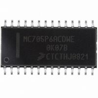
MC705P6ACDWE Freescale Semiconductor, MC705P6ACDWE Datasheet - Page 16

MC705P6ACDWE
Manufacturer Part Number
MC705P6ACDWE
Description
IC MCU 176 BYTES RAM 28-SOIC
Manufacturer
Freescale Semiconductor
Series
HC05r
Datasheet
1.MC705P6ACDWE.pdf
(98 pages)
Specifications of MC705P6ACDWE
Core Processor
HC05
Core Size
8-Bit
Speed
2.1MHz
Connectivity
SIO
Peripherals
POR, WDT
Number Of I /o
21
Program Memory Size
4.5KB (4.5K x 8)
Program Memory Type
OTP
Ram Size
176 x 8
Voltage - Supply (vcc/vdd)
3 V ~ 5.5 V
Data Converters
A/D 4x8b
Oscillator Type
Internal
Operating Temperature
-40°C ~ 85°C
Package / Case
28-SOIC (7.5mm Width)
Processor Series
HC705P
Core
HC05
Data Bus Width
8 bit
Data Ram Size
176 B
Maximum Clock Frequency
2.1 MHz
Number Of Programmable I/os
21
Number Of Timers
1
Maximum Operating Temperature
+ 85 C
Mounting Style
SMD/SMT
Minimum Operating Temperature
- 40 C
On-chip Adc
8 bit, 4 Channel
Lead Free Status / RoHS Status
Lead free / RoHS Compliant
Eeprom Size
-
Lead Free Status / Rohs Status
Details
Available stocks
Company
Part Number
Manufacturer
Quantity
Price
Company:
Part Number:
MC705P6ACDWE
Manufacturer:
Freescale Semiconductor
Quantity:
135
Part Number:
MC705P6ACDWE
Manufacturer:
FREESCALE
Quantity:
20 000
General Description
1.3.2.1 Crystal
The circuit in
Figure
1-2(a) shows a typical oscillator circuit for an AT-cut, parallel resonant crystal. Follow
the crystal manufacturer’s recommendations, as the crystal parameters determine the external
component values required to provide maximum stability and reliable startup. The load capacitance
values used in the oscillator circuit design should include all stray capacitances. Mount the crystal and
components as close as possible to the pins for startup stabilization and to minimize output distortion.
1.3.2.2 Ceramic Resonator
In cost-sensitive applications, use a ceramic resonator in place of a crystal. Use the circuit in
Figure
1-2(a)
for a ceramic resonator and follow the resonator manufacturer’s recommendations, as the resonator
parameters determine the external component values required for maximum stability and reliable starting.
The load capacitance values used in the oscillator circuit design should include all stray capacitances.
Mount the resonator and components as close as possible to the pins for startup stabilization and to
minimize output distortion.
1.3.2.3 External Clock
An external clock from another CMOS-compatible device can be connected to the OSC1 input, with the
OSC2 input not connected, as shown in
Figure
1-2(b).
1.3.3 RESET
Driving this input low will reset the MCU to a known startup state. The RESET pin contains an internal
Schmitt trigger to improve its noise immunity. Refer to
Chapter 4
Resets.
1.3.4 PA0–PA7
These eight I/O pins comprise port A. The state of any pin is software programmable and all port A lines
are configured as inputs during power-on or reset. Port A has mask-option register enabled interrupt
capability with internal pullup devices selectable for any pin. Refer to
Chapter 6 Input/Output
Ports.
1.3.5 PB5/SDO, PB6/SDI, and PB7/SCK
These three I/O pins comprise port B and are shared with the SIOP communications subsystem. The
state of any pin is software programmable, and all port B lines are configured as inputs during power-on
or reset. Refer to
Chapter 6 Input/Output Ports
and
Chapter 7 Serial Input/Output Port
(SIOP).
1.3.6 PC0-PC2, PC3/AD3, PC4/AD2, PC5/AD1, PC6/AD0, and PC7/V
REFH
These eight I/O pins comprise port C and are shared with the A/D converter subsystem. The state of any
pin is software programmable and all port C lines are configured as inputs during power-on or reset. Refer
to
Chapter 6 Input/Output Ports
and
Chapter 9 Analog
Subsystem.
1.3.7 PD5 and PD7/TCAP
These two I/O pins comprise port D and one of them is shared with the 16-bit timer subsystem. The state
of PD5 is software programmable and is configured as an input during power-on or reset. PD7 is always
an input. It may be read at any time, regardless of which mode of operation the 16-bit timer is in. Refer to
Chapter 6 Input/Output Ports
and
Chapter 8 Capture/Compare
Timer.
MC68HC705P6A Advance Information Data Sheet, Rev. 2.1
16
Freescale Semiconductor


