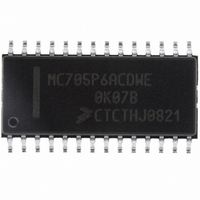
MC705P6ACDWE Freescale Semiconductor, MC705P6ACDWE Datasheet - Page 15

MC705P6ACDWE
Manufacturer Part Number
MC705P6ACDWE
Description
IC MCU 176 BYTES RAM 28-SOIC
Manufacturer
Freescale Semiconductor
Series
HC05r
Datasheet
1.MC705P6ACDWE.pdf
(98 pages)
Specifications of MC705P6ACDWE
Core Processor
HC05
Core Size
8-Bit
Speed
2.1MHz
Connectivity
SIO
Peripherals
POR, WDT
Number Of I /o
21
Program Memory Size
4.5KB (4.5K x 8)
Program Memory Type
OTP
Ram Size
176 x 8
Voltage - Supply (vcc/vdd)
3 V ~ 5.5 V
Data Converters
A/D 4x8b
Oscillator Type
Internal
Operating Temperature
-40°C ~ 85°C
Package / Case
28-SOIC (7.5mm Width)
Processor Series
HC705P
Core
HC05
Data Bus Width
8 bit
Data Ram Size
176 B
Maximum Clock Frequency
2.1 MHz
Number Of Programmable I/os
21
Number Of Timers
1
Maximum Operating Temperature
+ 85 C
Mounting Style
SMD/SMT
Minimum Operating Temperature
- 40 C
On-chip Adc
8 bit, 4 Channel
Lead Free Status / RoHS Status
Lead free / RoHS Compliant
Eeprom Size
-
Lead Free Status / Rohs Status
Details
Available stocks
Company
Part Number
Manufacturer
Quantity
Price
Company:
Part Number:
MC705P6ACDWE
Manufacturer:
Freescale Semiconductor
Quantity:
135
Part Number:
MC705P6ACDWE
Manufacturer:
FREESCALE
Quantity:
20 000
1.3 Functional Pin Description
The following paragraphs describe the functionality of each pin on the MC68HC705P6A package. Pins
connected to subsystems described in other chapters provide a reference to the chapter instead of a
detailed functional description.
1.3.1 V
Power is supplied to the MCU through V
V
Very fast signal transitions occur on the MCU pins. The short rise and fall times place very high
short-duration current demands on the power supply. To prevent noise problems, take special care to
provide good power supply bypassing at the MCU. Use bypass capacitors with good high-frequency
characteristics and position them as close to the MCU as possible. Bypassing requirements vary,
depending on how heavily the MCU pins are loaded.
1.3.2 OSC1 and OSC2
The OSC1 and OSC2 pins are the control connections for the on-chip oscillator. The OSC1 and OSC2
pins can accept the following:
The frequency, f
clock operating frequency, f
is clear when a STOP instruction is executed.
Freescale Semiconductor
SS
1. A crystal as shown in
2. A ceramic resonator as shown in
3. An external clock signal as shown in
is connected to ground.
DD
and V
osc
SS
, of the oscillator or external clock source is divided by two to produce the internal bus
(a)
To V
OSC1
37 pF
DD
Crystal or Ceramic
Resonator Connections
(or STOP)
MC68HC705P6A Advance Information Data Sheet, Rev. 2.1
op
4.7 MΩ
Figure
. The oscillator cannot be turned off by software unless the MOR bit, SWAIT,
Figure 1-2. Oscillator Connections
1-2(a)
OSC2
37 pF
DD
Figure
MCU
and V
Figure
1-2(a)
SS
1-2(b)
. V
DD
is connected to a regulated +5 volt supply and
To V
(b)
OSC1
DD
(or STOP)
External Clock Source
Connections
UNCONNECTED
EXTERNAL CLOCK
OSC2
MCU
Functional Pin Description
15


