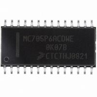
MC705P6ACDWE Freescale Semiconductor, MC705P6ACDWE Datasheet - Page 54

MC705P6ACDWE
Manufacturer Part Number
MC705P6ACDWE
Description
IC MCU 176 BYTES RAM 28-SOIC
Manufacturer
Freescale Semiconductor
Series
HC05r
Datasheet
1.MC705P6ACDWE.pdf
(98 pages)
Specifications of MC705P6ACDWE
Core Processor
HC05
Core Size
8-Bit
Speed
2.1MHz
Connectivity
SIO
Peripherals
POR, WDT
Number Of I /o
21
Program Memory Size
4.5KB (4.5K x 8)
Program Memory Type
OTP
Ram Size
176 x 8
Voltage - Supply (vcc/vdd)
3 V ~ 5.5 V
Data Converters
A/D 4x8b
Oscillator Type
Internal
Operating Temperature
-40°C ~ 85°C
Package / Case
28-SOIC (7.5mm Width)
Processor Series
HC705P
Core
HC05
Data Bus Width
8 bit
Data Ram Size
176 B
Maximum Clock Frequency
2.1 MHz
Number Of Programmable I/os
21
Number Of Timers
1
Maximum Operating Temperature
+ 85 C
Mounting Style
SMD/SMT
Minimum Operating Temperature
- 40 C
On-chip Adc
8 bit, 4 Channel
Lead Free Status / RoHS Status
Lead free / RoHS Compliant
Eeprom Size
-
Lead Free Status / Rohs Status
Details
Available stocks
Company
Part Number
Manufacturer
Quantity
Price
Company:
Part Number:
MC705P6ACDWE
Manufacturer:
Freescale Semiconductor
Quantity:
135
Part Number:
MC705P6ACDWE
Manufacturer:
FREESCALE
Quantity:
20 000
Analog Subsystem
9.4.1 Conversion Times
Each input conversion requires 32 internal clock cycles, which must be at a frequency equal to or greater
than 1 MHz.
9.4.2 Internal versus External Oscillator
If the internal clock is 1 MHz or greater (i.e., external oscillator 2 MHz or greater), the internal RC oscillator
must be turned off and the external oscillator used as the conversion clock.
If the MCU internal clock frequency is less than 1 MHz (2 MHz external oscillator), the internal RC
oscillator (approximately 1.5 MHz) must be used for the A/D converter clock. The internal RC clock is
selected by setting the ADRC bit in the ADSC register.
When the internal RC oscillator is being used, these limitations apply:
9.4.3 Multi-Channel Operation
An input multiplexer allows the A/D converter to select from one of four external analog signals. Port C
pins PC3 through PC6 are shared with the inputs to the multiplexer.
9.5 A/D Status and Control Register (ADSC)
The ADSC register reports the completion of A/D conversion and provides control over oscillator
selection, analog subsystem power, and input channel selection. See
CC — Conversion Complete
54
1. Since the internal RC oscillator is running asynchronously with respect to the internal clock, the
2. Electrical noise will slightly degrade the accuracy of the A/D converter. The A/D converter is
This read-only status bit is set when a conversion sequence has completed and data is ready to be
read from the ADC register. CC is cleared when the ADSC is written to or when data is read from the
ADC register. Once a conversion has been started, conversions of the selected channel will continue
every 32 internal clock cycles until the ADSC register is written to again. During continuous conversion
operation, the ADC register will be updated with new data, and the CC bit set every 32 internal clock
cycles. Also, data from the previous conversion will be overwritten regardless of the state of the CC bit.
conversion complete bit (CC) in register ADSC must be used to determine when a conversion
sequence has been completed.
synchronized to read voltages during the quiet period of the clock driving it. Since the internal and
external clocks are not synchronized, the A/D converter will occasionally measure an input when
the external clock is making a transition.
Address: $001E
Reset:
Read:
Write:
Bit 7
CC
Figure 9-1. A/D Status and Control Register (ADSC)
0
MC68HC705P6A Advance Information Data Sheet, Rev. 2.1
= Unimplemented
ADRC
6
0
ADON
5
0
4
0
0
3
0
0
CH2
2
0
Figure
9-1.
CH1
1
0
Freescale Semiconductor
Bit 0
CH0
0


