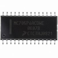
MC705P6ACDWE Freescale Semiconductor, MC705P6ACDWE Datasheet - Page 43

MC705P6ACDWE
Manufacturer Part Number
MC705P6ACDWE
Description
IC MCU 176 BYTES RAM 28-SOIC
Manufacturer
Freescale Semiconductor
Series
HC05r
Datasheet
1.MC705P6ACDWE.pdf
(98 pages)
Specifications of MC705P6ACDWE
Core Processor
HC05
Core Size
8-Bit
Speed
2.1MHz
Connectivity
SIO
Peripherals
POR, WDT
Number Of I /o
21
Program Memory Size
4.5KB (4.5K x 8)
Program Memory Type
OTP
Ram Size
176 x 8
Voltage - Supply (vcc/vdd)
3 V ~ 5.5 V
Data Converters
A/D 4x8b
Oscillator Type
Internal
Operating Temperature
-40°C ~ 85°C
Package / Case
28-SOIC (7.5mm Width)
Processor Series
HC705P
Core
HC05
Data Bus Width
8 bit
Data Ram Size
176 B
Maximum Clock Frequency
2.1 MHz
Number Of Programmable I/os
21
Number Of Timers
1
Maximum Operating Temperature
+ 85 C
Mounting Style
SMD/SMT
Minimum Operating Temperature
- 40 C
On-chip Adc
8 bit, 4 Channel
Lead Free Status / RoHS Status
Lead free / RoHS Compliant
Eeprom Size
-
Lead Free Status / Rohs Status
Details
Available stocks
Company
Part Number
Manufacturer
Quantity
Price
Company:
Part Number:
MC705P6ACDWE
Manufacturer:
Freescale Semiconductor
Quantity:
135
Part Number:
MC705P6ACDWE
Manufacturer:
FREESCALE
Quantity:
20 000
7.3 SIOP Registers
The SIOP is programmed and controlled by the SIOP control register (SCR) located at address $000A,
the SIOP status register (SSR) located at address $000B, and the SIOP data register (SDR) located at
address $000C.
7.3.1 SIOP Control Register (SCR)
This register is located at address $000A and contains two bits.
in the register and indicates the value of each bit after reset.
SPE — Serial Peripheral Enable
MSTR — Master Mode Select
Freescale Semiconductor
When set, the SPE bit enables the SIOP subsystem such that SDO/PB5 is the serial data output,
SDI/PB6 is the serial data input, and SCK/PB7 is a serial clock input in the slave mode or a serial clock
output in the master mode. Port B DDR and data registers can be manipulated as usual (except for
PB5); however, these actions could affect the transmitted or received data.
The SPE bit is readable at any time. However, writing to the SIOP control register while a transmission
is in progress will cause the SPIF and DCOL bits in the SIOP status register (see below) to operate
incorrectly. Therefore, the SIOP control register should be written once to enable the SIOP and then
not written to until the SIOP is to be disabled. Clearing the SPE bit while a transmission is in progress
will 1) abort the transmission, 2) reset the serial bit counter, and 3) convert the port B/SIOP port to a
general-purpose I/O port. Reset clears the SPE bit.
When set, the MSTR bit configures the serial I/O port for master mode. A transfer is initiated by writing
to the SDR. Also, the SCK pin becomes an output providing a synchronous data clock dependent upon
the oscillator frequency. When the device is in slave mode, the SDO and SDI pins do not change
function. These pins behave exactly the same in both the master and slave modes.
The MSTR bit is readable and writeable at any time regardless of the state of the SPE bit. Clearing the
MSTR bit will abort any transfers that may have been in progress. Reset clears the MSTR bit as well
as the SPE bit, disabling the SIOP subsystem.
Address:
Reset:
Read:
Write:
$000A
Bit 7
0
0
MC68HC705P6A Advance Information Data Sheet, Rev. 2.1
= Unimplemented
Figure 7-3. SIOP Control Register (SCR)
SPE
6
0
5
0
0
MSTR
4
0
3
0
0
Figure 7-3
2
0
0
shows the position of each bit
1
0
0
Bit 0
0
0
SIOP Registers
43


