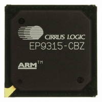
EP9315-CBZ Cirrus Logic Inc, EP9315-CBZ Datasheet - Page 783

EP9315-CBZ
Manufacturer Part Number
EP9315-CBZ
Description
IC ARM9 SOC ENH UNIV 352PBGA
Manufacturer
Cirrus Logic Inc
Series
EP9r
Specifications of EP9315-CBZ
Core Size
16/32-Bit
Core Processor
ARM9
Speed
200MHz
Connectivity
EBI/EMI, EIDE, Ethernet, I²C, IrDA, Keypad/Touchscreen, PCMCIA, SPI, UART/USART, USB
Peripherals
AC'97, DMA, I²:S, LCD, LED, MaverickKey, POR, PWM, WDT
Number Of I /o
16
Program Memory Type
ROMless
Ram Size
32K x 8
Voltage - Supply (vcc/vdd)
1.65 V ~ 3.6 V
Data Converters
A/D 8x12b
Oscillator Type
External
Operating Temperature
0°C ~ 70°C
Package / Case
352-BGA
Controller Family/series
(ARM9)
No. Of I/o's
16
Cpu Speed
200MHz
No. Of Timers
5
Digital Ic Case Style
BGA
Supply Voltage Range
1.65V To 1.94V, 3V To 3.6V
Embedded Interface Type
SPI
Rohs Compliant
Yes
Processor Series
EP93xx
Core
ARM920T
Data Bus Width
32 bit
3rd Party Development Tools
MDK-ARM, RL-ARM, ULINK2
Development Tools By Supplier
EDB9315A-Z
Case
BGA
Dc
06+
Lead Free Status / RoHS Status
Lead free / RoHS Compliant
For Use With
598-1144 - KIT DEVELOPMENT EP9315 ARM9
Eeprom Size
-
Program Memory Size
-
Lead Free Status / Rohs Status
Details
Other names
598-1139
Available stocks
Company
Part Number
Manufacturer
Quantity
Price
Part Number:
EP9315-CBZ
Manufacturer:
CIRRUS
Quantity:
20 000
- Current page: 783 of 824
- Download datasheet (13Mb)
IDEDataOut
DS785UM1
31
15
Default:
Definition:
Bit Descriptions:
Address:
Default:
Definition:
Bit Descriptions:
Note: Before setting the UEN bit to enable UDMA operation:
30
14
1 - Set or Clear the RWOP bit to configure for a Write or Read operation.
2 - Perform a dummy read of the IDEUDMAOp register.
3 - Set the UEN bit to enable UDMA operation.
29
13
28
12
0x0000_0000
IDE UDMA Configuration Register.
RSVD:
RWOP:
UEN:
0x800A_0010 - Read/Write
0x0000_0000
In PIO mode write operation, this register is the Output Data Registers,
containing the register contents or the data to be written to the device. The
register is driven onto the DD pins when DIOWn is low. The register is both
read write in this operation. In MDMA and UDMA data-out operations, this
register is an exact copy of the data in the output buffer to be transferred to the
device. The register should only be read in these operations for checking the
output data. Any write in these two operation modes is ignored.
IDEDD:
27
11
26
10
Copyright 2007 Cirrus Logic
25
9
Reserved. Unknown during read, ignored during write.
Read or write operation selection:
0 - Read
1 - Write.
Enable Ultra DMA operation.
1 - to start UDMA
0 - to terminate UDMA by the host.
IDE output data in PIO writes (read write), data in output
buffer in MDMA and data at the tail of output buffer in
UDMA mode (read only).
24
8
IDEDD
IDEDD
23
7
22
6
21
5
20
4
19
3
EP93xx User’s Guide
18
2
IDE Interface
17
1
27-13
16
0
27
Related parts for EP9315-CBZ
Image
Part Number
Description
Manufacturer
Datasheet
Request
R

Part Number:
Description:
IC ARM920T MCU 200MHZ 352-PBGA
Manufacturer:
Cirrus Logic Inc
Datasheet:

Part Number:
Description:
32-Bit Microcontroller IC
Manufacturer:
Cirrus Logic Inc
Datasheet:

Part Number:
Description:
IC ARM920T MCU 200MHZ 352-PBGA
Manufacturer:
Cirrus Logic Inc
Datasheet:

Part Number:
Description:
MCU, MPU & DSP Development Tools Eval Bd Uni. ARM9 SOC Processor
Manufacturer:
Cirrus Logic Inc
Datasheet:

Part Number:
Description:
Development Kit
Manufacturer:
Cirrus Logic Inc
Datasheet:

Part Number:
Description:
Development Kit
Manufacturer:
Cirrus Logic Inc
Datasheet:

Part Number:
Description:
High-efficiency PFC + Fluorescent Lamp Driver Reference Design
Manufacturer:
Cirrus Logic Inc
Datasheet:

Part Number:
Description:
Development Kit
Manufacturer:
Cirrus Logic Inc
Datasheet:

Part Number:
Description:
Development Kit
Manufacturer:
Cirrus Logic Inc
Datasheet:

Part Number:
Description:
Development Kit
Manufacturer:
Cirrus Logic Inc
Datasheet:

Part Number:
Description:
Development Kit
Manufacturer:
Cirrus Logic Inc
Datasheet:

Part Number:
Description:
Development Kit
Manufacturer:
Cirrus Logic Inc
Datasheet:

Part Number:
Description:
Development Kit
Manufacturer:
Cirrus Logic Inc
Datasheet:

Part Number:
Description:
Ref Bd For Speakerbar MSA & DSP Products
Manufacturer:
Cirrus Logic Inc


