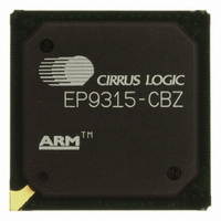
EP9315-CBZ Cirrus Logic Inc, EP9315-CBZ Datasheet - Page 607

EP9315-CBZ
Manufacturer Part Number
EP9315-CBZ
Description
IC ARM9 SOC ENH UNIV 352PBGA
Manufacturer
Cirrus Logic Inc
Series
EP9r
Specifications of EP9315-CBZ
Core Size
16/32-Bit
Core Processor
ARM9
Speed
200MHz
Connectivity
EBI/EMI, EIDE, Ethernet, I²C, IrDA, Keypad/Touchscreen, PCMCIA, SPI, UART/USART, USB
Peripherals
AC'97, DMA, I²:S, LCD, LED, MaverickKey, POR, PWM, WDT
Number Of I /o
16
Program Memory Type
ROMless
Ram Size
32K x 8
Voltage - Supply (vcc/vdd)
1.65 V ~ 3.6 V
Data Converters
A/D 8x12b
Oscillator Type
External
Operating Temperature
0°C ~ 70°C
Package / Case
352-BGA
Controller Family/series
(ARM9)
No. Of I/o's
16
Cpu Speed
200MHz
No. Of Timers
5
Digital Ic Case Style
BGA
Supply Voltage Range
1.65V To 1.94V, 3V To 3.6V
Embedded Interface Type
SPI
Rohs Compliant
Yes
Processor Series
EP93xx
Core
ARM920T
Data Bus Width
32 bit
3rd Party Development Tools
MDK-ARM, RL-ARM, ULINK2
Development Tools By Supplier
EDB9315A-Z
Case
BGA
Dc
06+
Lead Free Status / RoHS Status
Lead free / RoHS Compliant
For Use With
598-1144 - KIT DEVELOPMENT EP9315 ARM9
Eeprom Size
-
Program Memory Size
-
Lead Free Status / Rohs Status
Details
Other names
598-1139
Available stocks
Company
Part Number
Manufacturer
Quantity
Price
Part Number:
EP9315-CBZ
Manufacturer:
CIRRUS
Quantity:
20 000
- Current page: 607 of 824
- Download datasheet (13Mb)
DS785UM1
17.4.2 Functional Description
17.4.2.1 Baud Rate Generation
17.4.2.2 Receive Operation
Following reset, the MIR is disabled. Reset also causes the transmit and receive buffers and
tail register to be flushed (buffers marked as empty). To transmit data in MIR mode, use the
following procedure:
The baud or bit rate is derived by dividing down an 18.423MHz clock. The clock is divided
down by either 1 (BRD=1) or 2 (BRD=0) and then by a fixed value of four, generating the
transmit clock for 1.152Mb/s and 0.576Mb/s data rates, respectively. The receive clock is
generated by the receiver Digital Phase Locked Loop (DPLL). The DPLL uses a sample clock
that is undivided. A sample rate counter (incremented at the sample clock rate) is used to
generate a receive clock at the nominal data rate (sample clock divided by 41 and two-thirds).
The sample rate counter is reset on the detection of each positive-going data transition
(indicating the RZI encoding of a “0”) to ensure that synchronization with the incoming data
stream is maintained.
Once the MIR receiver is enabled it enters hunt mode, searching the incoming data stream
for the flag (01111110b). The flag serves to achieve bit synchronization, denotes the
beginning of a frame and delineates the boundaries of individual bytes of data. The end of the
second flag denotes the beginning of the address byte. Once the flag is found, the receiver is
synchronized to incoming data and hunt mode is exited.
After each bit is decoded, a serial shifter is used to receive the incoming data a byte at a time.
Once the flag is recognized, each subsequent byte of data is decoded and placed within a
two byte temporary buffer. A temporary buffer is used to prevent the CRC from being placed
within the receive buffer. When the temporary buffer is filled, data values are pushed out one
by one to the receive buffer. The first byte of a frame is the address. If receiver address
matching is enabled, the received address is compared to the address programmed in the
address match value field in a control register. If the two values are equal or if the incoming
address contains all ones, all subsequent data bytes including the address byte are stored in
the receive buffer. If the values do not match, the receive logic does not store any data in the
1. Set the EN bits in the IrEnable register to 10b for MIR mode. Do not begin data
2. Before enabling the MIR, the user must first clear any writable or “sticky” status bits that
3. Next, the desired mode of operation is programmed in the control register. Set the TXE
4. Write 1 to 3 bytes to the appropriate IrDataTail register.
5. Once the MIR is enabled, transmission/reception of data can begin on the transmit and
transmission.
are set by writing a one to each bit. (A sticky bit is a readable status bit that may be
cleared by writing a one to its location.) Set the TAB and TFC bits in the MISR register,
then read the MISR register to clear all interrupts.
and RXE bits in the IrCtrl register.
receive pins.
Copyright 2007 Cirrus Logic
EP93xx User’s Guide
17-11
IrDA
17
Related parts for EP9315-CBZ
Image
Part Number
Description
Manufacturer
Datasheet
Request
R

Part Number:
Description:
IC ARM920T MCU 200MHZ 352-PBGA
Manufacturer:
Cirrus Logic Inc
Datasheet:

Part Number:
Description:
32-Bit Microcontroller IC
Manufacturer:
Cirrus Logic Inc
Datasheet:

Part Number:
Description:
IC ARM920T MCU 200MHZ 352-PBGA
Manufacturer:
Cirrus Logic Inc
Datasheet:

Part Number:
Description:
MCU, MPU & DSP Development Tools Eval Bd Uni. ARM9 SOC Processor
Manufacturer:
Cirrus Logic Inc
Datasheet:

Part Number:
Description:
Development Kit
Manufacturer:
Cirrus Logic Inc
Datasheet:

Part Number:
Description:
Development Kit
Manufacturer:
Cirrus Logic Inc
Datasheet:

Part Number:
Description:
High-efficiency PFC + Fluorescent Lamp Driver Reference Design
Manufacturer:
Cirrus Logic Inc
Datasheet:

Part Number:
Description:
Development Kit
Manufacturer:
Cirrus Logic Inc
Datasheet:

Part Number:
Description:
Development Kit
Manufacturer:
Cirrus Logic Inc
Datasheet:

Part Number:
Description:
Development Kit
Manufacturer:
Cirrus Logic Inc
Datasheet:

Part Number:
Description:
Development Kit
Manufacturer:
Cirrus Logic Inc
Datasheet:

Part Number:
Description:
Development Kit
Manufacturer:
Cirrus Logic Inc
Datasheet:

Part Number:
Description:
Development Kit
Manufacturer:
Cirrus Logic Inc
Datasheet:

Part Number:
Description:
Ref Bd For Speakerbar MSA & DSP Products
Manufacturer:
Cirrus Logic Inc


