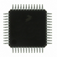
MC9S08DZ60ACLF Freescale Semiconductor, MC9S08DZ60ACLF Datasheet - Page 63

MC9S08DZ60ACLF
Manufacturer Part Number
MC9S08DZ60ACLF
Description
IC MCU 60K FLASH 4K RAM 48-LQFP
Manufacturer
Freescale Semiconductor
Series
HCS08r
Datasheets
1.DEMO9S08DZ60.pdf
(416 pages)
2.EVB9S08DZ60.pdf
(4 pages)
3.MC9S08DZ48AMLF.pdf
(458 pages)
Specifications of MC9S08DZ60ACLF
Core Processor
HCS08
Core Size
8-Bit
Speed
40MHz
Connectivity
CAN, I²C, LIN, SCI, SPI
Peripherals
LVD, POR, PWM, WDT
Number Of I /o
39
Program Memory Size
60KB (60K x 8)
Program Memory Type
FLASH
Eeprom Size
2K x 8
Ram Size
4K x 8
Voltage - Supply (vcc/vdd)
2.7 V ~ 5.5 V
Data Converters
A/D 16x12b
Oscillator Type
External
Operating Temperature
-40°C ~ 85°C
Package / Case
48-LQFP
Processor Series
S08DZ
Core
HCS08
Data Bus Width
8 bit
Data Ram Size
4 KB
Interface Type
CAN, I2C, SCI, SPI
Maximum Clock Frequency
40 MHz
Number Of Programmable I/os
53
Number Of Timers
2
Operating Supply Voltage
5.5 V
Maximum Operating Temperature
+ 85 C
Mounting Style
SMD/SMT
3rd Party Development Tools
EWS08
Development Tools By Supplier
DEMO9S08DZ60
Minimum Operating Temperature
- 40 C
On-chip Adc
12 bit, 24 Channel
For Use With
DEMO9S08DZ60 - BOARD DEMOEVB9S08DZ60 - BOARD EVAL FOR 9S08DZ60
Lead Free Status / RoHS Status
Lead free / RoHS Compliant
Available stocks
Company
Part Number
Manufacturer
Quantity
Price
Company:
Part Number:
MC9S08DZ60ACLF
Manufacturer:
FREESCAL
Quantity:
1 250
Company:
Part Number:
MC9S08DZ60ACLF
Manufacturer:
Freescale Semiconductor
Quantity:
10 000
- Current page: 63 of 458
- Download datasheet (5Mb)
Accessing either the LBP or LWP registers allows a user program to read successive memory locations
without re-writing the linear address pointer. Accessing LBP or LWP does the exact same function.
However, because of the address mapping of the registers with LBP following LWP, a user can do word
accesses in the extended address space using the LDHX or STHX instructions to access location LWP.
The MMU supports the addition of a 2s complement value to the linear address pointer without using any
math instructions or memory resources. Writes to LAPAB with a 2s complement value will cause the
MMU to add that value to the existing value in LAP2:LAP0.
4.4.3
4.4.3.1
The HCS08 Core architecture limits the CPU addressable space available to 64K bytes. The address space
can be extended to 128K bytes using a paging window scheme. The Program Page (PPAGE) allows for
selecting one of the 16K byte blocks to be accessed through the Program Page Window located at
0x8000-0xBFFF. The CALL and RTC instructions can load or store the value of PPAGE onto or from the
stack during program execution. After any reset, PPAGE is set to PAGE 2.
4.4.3.2
The three registers, LAP2:LAP0 contain the 17-bit linear address that allows the user to access any FLASH
location in the extended address map. This register is used in conjunction with the data registers, linear
byte (LB), linear byte post increment (LBP) and linear word post increment (LWP). The contents of
LAP2:LAP0 will auto-increment when accessing data using the LBP and LWP registers. The contents of
LAP2:LAP0 can be increased by writing an 8-bit value to LAPAB.
Freescale Semiconductor
XA16:XA14
Field
2:0
Reset:
MMU Registers and Control Bits
W
R
When the CPU addresses the paging window, 0x8000-0xBFFF, the value in the PPAGE register along with the
CPU addresses A13:A0 are used to create a 17-bit extended address.
Program Page Register (PPAGE)
Linear Address Pointer Registers 2:0 (LAP2:LAP0)
0
0
7
Table 4-6. Program Page Register Field Descriptions
0
0
6
Figure 4-5. Program Page Register (PPAGE)
MC9S08DZ128 Series Data Sheet, Rev. 1
5
0
0
0
0
4
Description
0
0
3
XA16
0
2
XA15
1
1
Chapter 4 Memory
XA14
0
0
63
Related parts for MC9S08DZ60ACLF
Image
Part Number
Description
Manufacturer
Datasheet
Request
R
Part Number:
Description:
Manufacturer:
Freescale Semiconductor, Inc
Datasheet:
Part Number:
Description:
Manufacturer:
Freescale Semiconductor, Inc
Datasheet:
Part Number:
Description:
Manufacturer:
Freescale Semiconductor, Inc
Datasheet:
Part Number:
Description:
Manufacturer:
Freescale Semiconductor, Inc
Datasheet:
Part Number:
Description:
Manufacturer:
Freescale Semiconductor, Inc
Datasheet:
Part Number:
Description:
Manufacturer:
Freescale Semiconductor, Inc
Datasheet:
Part Number:
Description:
Manufacturer:
Freescale Semiconductor, Inc
Datasheet:
Part Number:
Description:
Manufacturer:
Freescale Semiconductor, Inc
Datasheet:
Part Number:
Description:
Manufacturer:
Freescale Semiconductor, Inc
Datasheet:
Part Number:
Description:
Manufacturer:
Freescale Semiconductor, Inc
Datasheet:
Part Number:
Description:
Manufacturer:
Freescale Semiconductor, Inc
Datasheet:
Part Number:
Description:
Manufacturer:
Freescale Semiconductor, Inc
Datasheet:
Part Number:
Description:
Manufacturer:
Freescale Semiconductor, Inc
Datasheet:
Part Number:
Description:
Manufacturer:
Freescale Semiconductor, Inc
Datasheet:
Part Number:
Description:
Manufacturer:
Freescale Semiconductor, Inc
Datasheet:


