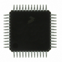
MC9S08DZ60ACLF Freescale Semiconductor, MC9S08DZ60ACLF Datasheet - Page 151

MC9S08DZ60ACLF
Manufacturer Part Number
MC9S08DZ60ACLF
Description
IC MCU 60K FLASH 4K RAM 48-LQFP
Manufacturer
Freescale Semiconductor
Series
HCS08r
Datasheets
1.DEMO9S08DZ60.pdf
(416 pages)
2.EVB9S08DZ60.pdf
(4 pages)
3.MC9S08DZ48AMLF.pdf
(458 pages)
Specifications of MC9S08DZ60ACLF
Core Processor
HCS08
Core Size
8-Bit
Speed
40MHz
Connectivity
CAN, I²C, LIN, SCI, SPI
Peripherals
LVD, POR, PWM, WDT
Number Of I /o
39
Program Memory Size
60KB (60K x 8)
Program Memory Type
FLASH
Eeprom Size
2K x 8
Ram Size
4K x 8
Voltage - Supply (vcc/vdd)
2.7 V ~ 5.5 V
Data Converters
A/D 16x12b
Oscillator Type
External
Operating Temperature
-40°C ~ 85°C
Package / Case
48-LQFP
Processor Series
S08DZ
Core
HCS08
Data Bus Width
8 bit
Data Ram Size
4 KB
Interface Type
CAN, I2C, SCI, SPI
Maximum Clock Frequency
40 MHz
Number Of Programmable I/os
53
Number Of Timers
2
Operating Supply Voltage
5.5 V
Maximum Operating Temperature
+ 85 C
Mounting Style
SMD/SMT
3rd Party Development Tools
EWS08
Development Tools By Supplier
DEMO9S08DZ60
Minimum Operating Temperature
- 40 C
On-chip Adc
12 bit, 24 Channel
For Use With
DEMO9S08DZ60 - BOARD DEMOEVB9S08DZ60 - BOARD EVAL FOR 9S08DZ60
Lead Free Status / RoHS Status
Lead free / RoHS Compliant
Available stocks
Company
Part Number
Manufacturer
Quantity
Price
Company:
Part Number:
MC9S08DZ60ACLF
Manufacturer:
FREESCAL
Quantity:
1 250
Company:
Part Number:
MC9S08DZ60ACLF
Manufacturer:
Freescale Semiconductor
Quantity:
10 000
- Current page: 151 of 458
- Download datasheet (5Mb)
while the CPU is in stop mode, CPU clocks will resume and the CPU will enter active background mode
where other serial background commands can be processed. This ensures that a host development system
can still gain access to a target MCU even if it is in stop mode.
Recovery from stop mode depends on the particular HCS08 and whether the oscillator was stopped in stop
mode. Refer to the
7.4.5
The BGND instruction is new to the HCS08 compared to the M68HC08. BGND would not be used in
normal user programs because it forces the CPU to stop processing user instructions and enter the active
background mode. The only way to resume execution of the user program is through reset or by a host
debug system issuing a GO, TRACE1, or TAGGO serial command through the background debug
interface.
Software-based breakpoints can be set by replacing an opcode at the desired breakpoint address with the
BGND opcode. When the program reaches this breakpoint address, the CPU is forced to active background
mode rather than continuing the user program.
7.5
The CALL is similar to a jump-to-subroutine (JSR) instruction, but the subroutine that is called can be
located anywhere in the normal 64-Kbyte address space or on any page of program expansion memory.
When CALL is executed, a return address is calculated, then it and the current program page register value
are stacked, and a new instruction-supplied value is written to PPAGE. The PPAGE value controls which
of the possible 16-Kbyte pages is visible through the window in the 64-Kbyte memory map. Execution
continues at the address of the called subroutine.
The actual sequence of operations that occur during execution of CALL is:
This sequence of operations is an uninterruptable CPU instruction. There is no need to inhibit interrupts
during CALL execution. In addition, a CALL can be performed from any address in memory to any other
address. This is a big improvement over other bank-switching schemes, where the page switch operation
can be performed only by a program outside the overlay window.
For all practical purposes, the PPAGE value supplied by the instruction can be considered to be part of the
effective address. The new page value is provided by an immediate operand in the instruction.
Freescale Semiconductor
1. CPU calculates the address of the next instruction after the CALL instruction (the return address)
2. CPU reads the old PPAGE value and pushes it onto the stack.
3. CPU writes the new instruction-supplied page select value to PPAGE. This switches the destination
4. Instruction queue is refilled starting from the destination address, and execution begins at the new
and pushes this 16-bit value onto the stack, low byte first.
page into the program overlay window in the CPU address range 0x8000 0xBFFF.
address.
CALL and RTC Instructions
BGND Instruction
Modes of Operation
MC9S08DZ128 Series Data Sheet, Rev. 1
chapter for more details.
Chapter 7 Central Processor Unit (S08CPUV5)
151
Related parts for MC9S08DZ60ACLF
Image
Part Number
Description
Manufacturer
Datasheet
Request
R
Part Number:
Description:
Manufacturer:
Freescale Semiconductor, Inc
Datasheet:
Part Number:
Description:
Manufacturer:
Freescale Semiconductor, Inc
Datasheet:
Part Number:
Description:
Manufacturer:
Freescale Semiconductor, Inc
Datasheet:
Part Number:
Description:
Manufacturer:
Freescale Semiconductor, Inc
Datasheet:
Part Number:
Description:
Manufacturer:
Freescale Semiconductor, Inc
Datasheet:
Part Number:
Description:
Manufacturer:
Freescale Semiconductor, Inc
Datasheet:
Part Number:
Description:
Manufacturer:
Freescale Semiconductor, Inc
Datasheet:
Part Number:
Description:
Manufacturer:
Freescale Semiconductor, Inc
Datasheet:
Part Number:
Description:
Manufacturer:
Freescale Semiconductor, Inc
Datasheet:
Part Number:
Description:
Manufacturer:
Freescale Semiconductor, Inc
Datasheet:
Part Number:
Description:
Manufacturer:
Freescale Semiconductor, Inc
Datasheet:
Part Number:
Description:
Manufacturer:
Freescale Semiconductor, Inc
Datasheet:
Part Number:
Description:
Manufacturer:
Freescale Semiconductor, Inc
Datasheet:
Part Number:
Description:
Manufacturer:
Freescale Semiconductor, Inc
Datasheet:
Part Number:
Description:
Manufacturer:
Freescale Semiconductor, Inc
Datasheet:


