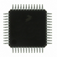
MC9S08DZ60ACLF Freescale Semiconductor, MC9S08DZ60ACLF Datasheet - Page 177

MC9S08DZ60ACLF
Manufacturer Part Number
MC9S08DZ60ACLF
Description
IC MCU 60K FLASH 4K RAM 48-LQFP
Manufacturer
Freescale Semiconductor
Series
HCS08r
Datasheets
1.DEMO9S08DZ60.pdf
(416 pages)
2.EVB9S08DZ60.pdf
(4 pages)
3.MC9S08DZ48AMLF.pdf
(458 pages)
Specifications of MC9S08DZ60ACLF
Core Processor
HCS08
Core Size
8-Bit
Speed
40MHz
Connectivity
CAN, I²C, LIN, SCI, SPI
Peripherals
LVD, POR, PWM, WDT
Number Of I /o
39
Program Memory Size
60KB (60K x 8)
Program Memory Type
FLASH
Eeprom Size
2K x 8
Ram Size
4K x 8
Voltage - Supply (vcc/vdd)
2.7 V ~ 5.5 V
Data Converters
A/D 16x12b
Oscillator Type
External
Operating Temperature
-40°C ~ 85°C
Package / Case
48-LQFP
Processor Series
S08DZ
Core
HCS08
Data Bus Width
8 bit
Data Ram Size
4 KB
Interface Type
CAN, I2C, SCI, SPI
Maximum Clock Frequency
40 MHz
Number Of Programmable I/os
53
Number Of Timers
2
Operating Supply Voltage
5.5 V
Maximum Operating Temperature
+ 85 C
Mounting Style
SMD/SMT
3rd Party Development Tools
EWS08
Development Tools By Supplier
DEMO9S08DZ60
Minimum Operating Temperature
- 40 C
On-chip Adc
12 bit, 24 Channel
For Use With
DEMO9S08DZ60 - BOARD DEMOEVB9S08DZ60 - BOARD EVAL FOR 9S08DZ60
Lead Free Status / RoHS Status
Lead free / RoHS Compliant
Available stocks
Company
Part Number
Manufacturer
Quantity
Price
Company:
Part Number:
MC9S08DZ60ACLF
Manufacturer:
FREESCAL
Quantity:
1 250
Company:
Part Number:
MC9S08DZ60ACLF
Manufacturer:
Freescale Semiconductor
Quantity:
10 000
- Current page: 177 of 458
- Download datasheet (5Mb)
8.3.6
Freescale Semiconductor
dco_select
DMX32
DRST
Field
DRS
7:6
4:1
5
0
Reset:
W
R
MCG Test and Control Register (MCGT)
Reserved for test, user code should not write 1’s to these bits.
DCO Maximum frequency with 32.768 kHz reference — The DMX32 bit controls whether or not the DCO
frequency range is narrowed to its maximum frequency with a 32.768 kHz reference. See
0 DCO has default range of 25%.
1 DCO is fined tuned for maximum frequency with 32.768 kHz reference.
Reserved for test, user code should not write 1’s to these bits.
DCO Range Status — The DRST read bit indicates the current frequency range for the FLL output, DCOOUT.
See
synchronization between clock domains. The DRST bit is not valid in BLPI, BLPE, PBE or PEE mode and it reads
zero regardless of the DCO range selected by the DRS bit.
DCO Range Select — The DRS bit selects the frequency range for the FLL output, DCOOUT. Writes to the DRS
bit while either the LP or PLLS bit is set are ignored.
0 Low range.
1 Mid range.
Table
1
7
0
0
DRS DMX32
The resulting bus clock frequency should not exceed the maximum specified bus
clock frequency of the device.
0
1
8-9. The DRST bit does not update immediately after a write to the DRS field due to internal
Table 8-8. MCG Test and Control Register Field Descriptions
Figure 8-8. MCG Test and Control Register (MCGT)
0
1
0
1
0
0
6
31.25 - 39.0625 kHz
31.25 - 39.0625 kHz
MC9S08DZ128 Series Data Sheet, Rev. 1
Reference range
Table 8-9. DCO frequency range
DMX32
0
5
32.768 kHz
32.768 kHz
0
0
4
Description
FLL factor
1024
1216
512
608
Chapter 8 Multi-Purpose Clock Generator (S08MCGV2)
0
0
3
1
0
0
2
DCO range
16 - 20 MHz
32 - 40 MHz
19.92 MHz
39.85 MHz
0
0
1
Table
8-9.
DRST
DRS
1
0
177
Related parts for MC9S08DZ60ACLF
Image
Part Number
Description
Manufacturer
Datasheet
Request
R
Part Number:
Description:
Manufacturer:
Freescale Semiconductor, Inc
Datasheet:
Part Number:
Description:
Manufacturer:
Freescale Semiconductor, Inc
Datasheet:
Part Number:
Description:
Manufacturer:
Freescale Semiconductor, Inc
Datasheet:
Part Number:
Description:
Manufacturer:
Freescale Semiconductor, Inc
Datasheet:
Part Number:
Description:
Manufacturer:
Freescale Semiconductor, Inc
Datasheet:
Part Number:
Description:
Manufacturer:
Freescale Semiconductor, Inc
Datasheet:
Part Number:
Description:
Manufacturer:
Freescale Semiconductor, Inc
Datasheet:
Part Number:
Description:
Manufacturer:
Freescale Semiconductor, Inc
Datasheet:
Part Number:
Description:
Manufacturer:
Freescale Semiconductor, Inc
Datasheet:
Part Number:
Description:
Manufacturer:
Freescale Semiconductor, Inc
Datasheet:
Part Number:
Description:
Manufacturer:
Freescale Semiconductor, Inc
Datasheet:
Part Number:
Description:
Manufacturer:
Freescale Semiconductor, Inc
Datasheet:
Part Number:
Description:
Manufacturer:
Freescale Semiconductor, Inc
Datasheet:
Part Number:
Description:
Manufacturer:
Freescale Semiconductor, Inc
Datasheet:
Part Number:
Description:
Manufacturer:
Freescale Semiconductor, Inc
Datasheet:


