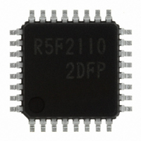
R5F21102DFP#U0 Renesas Electronics America, R5F21102DFP#U0 Datasheet - Page 198

R5F21102DFP#U0
Manufacturer Part Number
R5F21102DFP#U0
Description
IC R8C MCU FLASH 8K 32LQFP
Manufacturer
Renesas Electronics America
Series
M16C™ M16C/R8C/Tiny/10r
Datasheets
1.R5F211A2SPU0.pdf
(300 pages)
2.R5F21102FPU0.pdf
(30 pages)
3.R5F21102FPU0.pdf
(201 pages)
Specifications of R5F21102DFP#U0
Core Processor
R8C
Core Size
16-Bit
Speed
16MHz
Connectivity
SIO, UART/USART
Peripherals
LED, WDT
Number Of I /o
22
Program Memory Size
8KB (8K x 8)
Program Memory Type
FLASH
Ram Size
512 x 8
Voltage - Supply (vcc/vdd)
2.7 V ~ 5.5 V
Data Converters
A/D 8x10b
Oscillator Type
Internal
Operating Temperature
-40°C ~ 85°C
Package / Case
32-LQFP
For Use With
R0K521134S000BE - KIT EVAL STARTER FOR R8C/13R0E521134EPB00 - KIT EMULATOR PROBE FOR PC7501R0E521134CPE00 - EMULATOR COMPACT R8C/13
Lead Free Status / RoHS Status
Lead free / RoHS Compliant
Eeprom Size
-
Available stocks
Company
Part Number
Manufacturer
Quantity
Price
- Current page: 198 of 201
- Download datasheet (2Mb)
Rev.
1.20 Jan.27.2006
Date
REVISION HISTORY
Page
100
105
7-8
10
11
12
13
15
17
20
22
24
28
32
37
45
56
59
73
91
92
93
2
3
4
6
Table 1.1 Performance outline revised
Figure 1.1 Block diagram partly revised
1.4 Product Information, title of Table 1.2
“Product List”
Figure 1.2 Type No., Memory Size, and Package partly revised
Table 1.3 Pin description revised
2 Central Processing Unit (CPU) revised
Figure 2.1 CPU register revised
Table 4.1 SFR Information(1) NOTES:1 revised
Table 4.2 SFR Information(2) NOTES:1 revised
Table 4.3 SFR Information(3);
0081
0082
0083
0085
0086
0087
008C
NOTES:1 revised
Table 4.4 SFR Information(4) NOTES:1 revised
Figure 5.2 Reset Sequence; “72cycles”
6 Clock Generation Circuit;
“(oscillation stop detect function)”
Table 6.1 Clock Generation Circuit Specifications NOTES: 2 deleted
Figure 6.3 OCD Register NOTES: 3 partly deleted
6.2.1 On-Chip Oscillator Clock;
“The application products ... to accommodate the frequency range.”
“The application products ... for the frequency change.” revised
Table 6.2 Setting Clock Related Bit and Modes CM13 added
6.5.1 How to Use Oscillation Stop Detection Function:
“This function cannot ... is below 2 MHz.” added
Table 9.1 Bus Cycles for Access Space, Table 9.2 Access Unit and Bus Operation;
“SFR”
ROM/RAM”
Table 10.2 Relocatable Vector Tables; “A/D”
Figure 10.9 Interrupts Priority Select Circuit NOTES: 1 deleted
Figure 12.1 Timer X Block Diagram; “Peripheral data bus”
Table 12.3 Pulse Output Mode Specifications NOTES: 1 added
Figure 12.18 Timer Z Block Diagram; “Peripheral data bus”
Figure 13.3 U0TB to U1TB Registers, U0RB and U1RB Registers, and U0BRG and
U1BRG Registers;
UARTi transmit buffer register (i=0, 1) revised
UARTi bit rate register (i=0, 1); NOTES: 3 added
Figure 13.4 U0MR to U1MR Registers and U0C0 and U1C0 Registers;
UARTi transmit/receive control register 0 (i=0, 1); NOTES: 1 added
Figure 13.5 U0C1 and U1C1 Registers and UCON Register;
UART transmit/receive control register 2; NOTES: 2 added
Table 13.5 Registers to Be Used and Settings in UART Mode;
UiBRG: “–”
Figure 14.1 A/D Converter Block Diagram “Vref”
16
16
16
16
16
16
16
: “Prescaler Y”
: “Timer Y Secondary”
: “Timer Y Primary”
: “Prescaler Z”
: “Timer Z Secondary”
: “Timer Z Primary”
: “Prescaler X”
“SFR, Data flash”,
“0 to 7” revised
“Program ROM/RAM” revised
“Product Informaton” revised
C-6
“Prescaler Y Register”
“Prescaler Z Register”
“Prescaler X Register” revised
“Timer Y Primary Register”
“Timer Z Primary Register”
Description
R8C/10 Group Hardware Manual
“Timer Y Secondary Register”
“Timer Z Secondary Register”
Summary
“(oscillation stop detection function)” revised
“64cycles” revised
“A/D Conversion” revised
“Vcom” revised
“Data bus” revised
“Data bus” revised
Related parts for R5F21102DFP#U0
Image
Part Number
Description
Manufacturer
Datasheet
Request
R

Part Number:
Description:
KIT STARTER FOR M16C/29
Manufacturer:
Renesas Electronics America
Datasheet:

Part Number:
Description:
KIT STARTER FOR R8C/2D
Manufacturer:
Renesas Electronics America
Datasheet:

Part Number:
Description:
R0K33062P STARTER KIT
Manufacturer:
Renesas Electronics America
Datasheet:

Part Number:
Description:
KIT STARTER FOR R8C/23 E8A
Manufacturer:
Renesas Electronics America
Datasheet:

Part Number:
Description:
KIT STARTER FOR R8C/25
Manufacturer:
Renesas Electronics America
Datasheet:

Part Number:
Description:
KIT STARTER H8S2456 SHARPE DSPLY
Manufacturer:
Renesas Electronics America
Datasheet:

Part Number:
Description:
KIT STARTER FOR R8C38C
Manufacturer:
Renesas Electronics America
Datasheet:

Part Number:
Description:
KIT STARTER FOR R8C35C
Manufacturer:
Renesas Electronics America
Datasheet:

Part Number:
Description:
KIT STARTER FOR R8CL3AC+LCD APPS
Manufacturer:
Renesas Electronics America
Datasheet:

Part Number:
Description:
KIT STARTER FOR RX610
Manufacturer:
Renesas Electronics America
Datasheet:

Part Number:
Description:
KIT STARTER FOR R32C/118
Manufacturer:
Renesas Electronics America
Datasheet:

Part Number:
Description:
KIT DEV RSK-R8C/26-29
Manufacturer:
Renesas Electronics America
Datasheet:

Part Number:
Description:
KIT STARTER FOR SH7124
Manufacturer:
Renesas Electronics America
Datasheet:

Part Number:
Description:
KIT STARTER FOR H8SX/1622
Manufacturer:
Renesas Electronics America
Datasheet:

Part Number:
Description:
KIT DEV FOR SH7203
Manufacturer:
Renesas Electronics America
Datasheet:


