R5F21102DFP#U0 Renesas Electronics America, R5F21102DFP#U0 Datasheet - Page 10
R5F21102DFP#U0
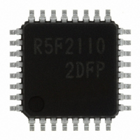
Manufacturer Part Number
R5F21102DFP#U0
Description
IC R8C MCU FLASH 8K 32LQFP
Manufacturer
Renesas Electronics America
Series
M16C™ M16C/R8C/Tiny/10r
Datasheets
1.R5F211A2SPU0.pdf
(300 pages)
2.R5F21102FPU0.pdf
(30 pages)
3.R5F21102FPU0.pdf
(201 pages)
Specifications of R5F21102DFP#U0
Core Processor
R8C
Core Size
16-Bit
Speed
16MHz
Connectivity
SIO, UART/USART
Peripherals
LED, WDT
Number Of I /o
22
Program Memory Size
8KB (8K x 8)
Program Memory Type
FLASH
Ram Size
512 x 8
Voltage - Supply (vcc/vdd)
2.7 V ~ 5.5 V
Data Converters
A/D 8x10b
Oscillator Type
Internal
Operating Temperature
-40°C ~ 85°C
Package / Case
32-LQFP
For Use With
R0K521134S000BE - KIT EVAL STARTER FOR R8C/13R0E521134EPB00 - KIT EMULATOR PROBE FOR PC7501R0E521134CPE00 - EMULATOR COMPACT R8C/13
Lead Free Status / RoHS Status
Lead free / RoHS Compliant
Eeprom Size
-
Available stocks
Company
Part Number
Manufacturer
Quantity
Price


Chapter 18. On-chip Debugger ........................................ 161
Chapter 19. Usage Notes .................................................. 162
Chapter 20. Usage Notes for On-chip Debugger ............ 174
Appendix 1 Package Dimensions .................................... 175
Appendix 2 Connecting Examples for Serial Writer and
On-chip Debugging Emulator .......................................... 176
Appendix 3 Example of Oscillation Evaluation Circuit .. 178
Register Index ................................................................... 179
18.1 Address Match Interrupt .......................................................................................... 161
18.2 Single Step Interrupt ................................................................................................ 161
18.3 UART1 ........................................................................................................................ 161
18.4 BRK Instrucstion ...................................................................................................... 161
19.1 Stop Mode and Wait Mode ....................................................................................... 162
19.2 Interrupts ................................................................................................................... 163
19.3 Clock Generation Circuit ......................................................................................... 166
19.4 Timers ........................................................................................................................ 167
19.5 Serial Interface .......................................................................................................... 168
19.6 A/D Converter............................................................................................................ 169
19.7 Flash Memory Version ............................................................................................. 170
19.8 Noise .......................................................................................................................... 173
19.1.1 Stop Mode .......................................................................................................................................... 162
19.1.2 Wait Mode .......................................................................................................................................... 162
19.2.1 Reading Address 00000
19.2.2 SP Setting .......................................................................................................................................... 163
19.2.3 External Interrupt and Key Input Interrupt ..................................................................................... 163
19.2.4 Watchdog Timer Interrupt ................................................................................................................ 163
19.2.5 Changing Interrupt Factor ................................................................................................................ 164
19.2.6 Changing Interrupt Control Register .............................................................................................. 165
19.3.1 Oscillation Stop Detection Function ............................................................................................... 166
19.3.2 Oscillation Circuit Constants ........................................................................................................... 166
19.3.1 Timers X, Y and Z .............................................................................................................................. 167
19.3.2 Timer X ............................................................................................................................................... 167
19.3.3 Timer Y ............................................................................................................................................... 167
19.3.4 Timer Z ............................................................................................................................................... 167
19.3.5 Timer C ............................................................................................................................................... 167
19.7.1 CPU Rewrite Mode ............................................................................................................................ 170
16 ............................................................................................................................................
A-4
163
Related parts for R5F21102DFP#U0
Image
Part Number
Description
Manufacturer
Datasheet
Request
R

Part Number:
Description:
KIT STARTER FOR M16C/29
Manufacturer:
Renesas Electronics America
Datasheet:

Part Number:
Description:
KIT STARTER FOR R8C/2D
Manufacturer:
Renesas Electronics America
Datasheet:

Part Number:
Description:
R0K33062P STARTER KIT
Manufacturer:
Renesas Electronics America
Datasheet:

Part Number:
Description:
KIT STARTER FOR R8C/23 E8A
Manufacturer:
Renesas Electronics America
Datasheet:

Part Number:
Description:
KIT STARTER FOR R8C/25
Manufacturer:
Renesas Electronics America
Datasheet:

Part Number:
Description:
KIT STARTER H8S2456 SHARPE DSPLY
Manufacturer:
Renesas Electronics America
Datasheet:

Part Number:
Description:
KIT STARTER FOR R8C38C
Manufacturer:
Renesas Electronics America
Datasheet:

Part Number:
Description:
KIT STARTER FOR R8C35C
Manufacturer:
Renesas Electronics America
Datasheet:

Part Number:
Description:
KIT STARTER FOR R8CL3AC+LCD APPS
Manufacturer:
Renesas Electronics America
Datasheet:
Part Number:
Description:
KIT STARTER FOR RX610
Manufacturer:
Renesas Electronics America
Datasheet:

Part Number:
Description:
KIT STARTER FOR R32C/118
Manufacturer:
Renesas Electronics America
Datasheet:

Part Number:
Description:
KIT DEV RSK-R8C/26-29
Manufacturer:
Renesas Electronics America
Datasheet:

Part Number:
Description:
KIT STARTER FOR SH7124
Manufacturer:
Renesas Electronics America
Datasheet:

Part Number:
Description:
KIT STARTER FOR H8SX/1622
Manufacturer:
Renesas Electronics America
Datasheet:

Part Number:
Description:
KIT DEV FOR SH7203
Manufacturer:
Renesas Electronics America
Datasheet: