R5F21102DFP#U0 Renesas Electronics America, R5F21102DFP#U0 Datasheet - Page 106
R5F21102DFP#U0
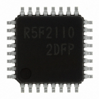
Manufacturer Part Number
R5F21102DFP#U0
Description
IC R8C MCU FLASH 8K 32LQFP
Manufacturer
Renesas Electronics America
Series
M16C™ M16C/R8C/Tiny/10r
Datasheets
1.R5F211A2SPU0.pdf
(300 pages)
2.R5F21102FPU0.pdf
(30 pages)
3.R5F21102FPU0.pdf
(201 pages)
Specifications of R5F21102DFP#U0
Core Processor
R8C
Core Size
16-Bit
Speed
16MHz
Connectivity
SIO, UART/USART
Peripherals
LED, WDT
Number Of I /o
22
Program Memory Size
8KB (8K x 8)
Program Memory Type
FLASH
Ram Size
512 x 8
Voltage - Supply (vcc/vdd)
2.7 V ~ 5.5 V
Data Converters
A/D 8x10b
Oscillator Type
Internal
Operating Temperature
-40°C ~ 85°C
Package / Case
32-LQFP
For Use With
R0K521134S000BE - KIT EVAL STARTER FOR R8C/13R0E521134EPB00 - KIT EMULATOR PROBE FOR PC7501R0E521134CPE00 - EMULATOR COMPACT R8C/13
Lead Free Status / RoHS Status
Lead free / RoHS Compliant
Eeprom Size
-
Available stocks
Company
Part Number
Manufacturer
Quantity
Price


R8C/10 Group
Rev.1.20 Jan 27, 2006
REJ09B0019-0120
13.1 Clock Synchronous Serial I/O Mode
Table 13.1 Clock Synchronous Serial I/O Mode Specifications
NOTES:
1. When an external clock is selected, the conditions must be met while if the U0C0 register 0 CKPOL bit
2. If an overrun error occurs, the value of U0RB register will be indeterminate. The IR bit of S0RIC register
Interrupt request
generation timing
Transfer data format
Transfer clock
Transmission start condition
Reception start condition
Error detection
Select function
The clock synchronous serial I/O mode uses a transfer clock to transmit and receive data. This mode can
be selected with UART0. Table 13.1 lists the specifications of the clock synchronous serial I/O mode.
Table 13.2 lists the registers used in clock synchronous serial I/O mode and the register values set.
= 0 (transmit data output at the falling edge and the receive data taken in at the rising edge of the
transfer clock), the external clock is in the high state; if the CKPOL bit in the U0C0 register is set to “1”
(transmit data output at the rising edge and the receive data taken in at the falling edge of the transfer
clock), the external clock is in the low state.
does not change.
Item
page 94 of 180
• Transfer data length: 8 bits
• CKDIR bit in U0MR register is set to “0” (internal clock): fi/(2(n+1))
• CKDIR bit is set to “1” (external clock ): input from CLK0 pin
• Before transmission can start, the following requirements must be met
_
_
• Before reception can start, the following requirements must be met
_
_
_
• For transmission, one of the following conditions can be selected
_
_
• For reception
• Overrun error
• CLK polarity selection
• LSB first, MSB first selection
• Continuous receive mode selection
When transferring data from the UART0 receive register to the U0RB register (at
completion of reception)
the falling edge of the transfer clock
fi=f
data from UARTi transmit register
This error occurs if serial interface started receiving the next data before reading the
U0RB register and received the 7th bit of the next data
Whether to start sending/receiving data beginning with bit 0 or beginning with bit 7
can be selected
Reception is enabled immediately by reading the U0RB register
TE bit in U0C1 register is set to “1” (transmission enabled)
TI bit in U0C1 register is set to “0” (data present in U0TB register)
RE bit in U0C1 register is set to “1” (reception enabled)
TE bit in U0C1 register is set to “1” (transmission enabled)
TI bit in U0C1 register is set to “0” (data present in the U0TB register)
U0IRS bit is set to “0” (transmit buffer empty): when transferring data from
U0IRS bit is set to “1” (transfer completed): when serial interface finished sending
U0TB register to UART0 transmit register (at start of transmission)
Transfer data I/O can be chosen to occur synchronously with the rising or
1SIO
, f
8SIO
, f
(2)
32SIO
n=setting value in UiBRG register: 00
Specification
13.1 Clock Synchronous Serial I/O Mode
16
to FF
(1)
16
(1)
Related parts for R5F21102DFP#U0
Image
Part Number
Description
Manufacturer
Datasheet
Request
R

Part Number:
Description:
KIT STARTER FOR M16C/29
Manufacturer:
Renesas Electronics America
Datasheet:

Part Number:
Description:
KIT STARTER FOR R8C/2D
Manufacturer:
Renesas Electronics America
Datasheet:

Part Number:
Description:
R0K33062P STARTER KIT
Manufacturer:
Renesas Electronics America
Datasheet:

Part Number:
Description:
KIT STARTER FOR R8C/23 E8A
Manufacturer:
Renesas Electronics America
Datasheet:

Part Number:
Description:
KIT STARTER FOR R8C/25
Manufacturer:
Renesas Electronics America
Datasheet:

Part Number:
Description:
KIT STARTER H8S2456 SHARPE DSPLY
Manufacturer:
Renesas Electronics America
Datasheet:

Part Number:
Description:
KIT STARTER FOR R8C38C
Manufacturer:
Renesas Electronics America
Datasheet:

Part Number:
Description:
KIT STARTER FOR R8C35C
Manufacturer:
Renesas Electronics America
Datasheet:

Part Number:
Description:
KIT STARTER FOR R8CL3AC+LCD APPS
Manufacturer:
Renesas Electronics America
Datasheet:
Part Number:
Description:
KIT STARTER FOR RX610
Manufacturer:
Renesas Electronics America
Datasheet:

Part Number:
Description:
KIT STARTER FOR R32C/118
Manufacturer:
Renesas Electronics America
Datasheet:

Part Number:
Description:
KIT DEV RSK-R8C/26-29
Manufacturer:
Renesas Electronics America
Datasheet:

Part Number:
Description:
KIT STARTER FOR SH7124
Manufacturer:
Renesas Electronics America
Datasheet:

Part Number:
Description:
KIT STARTER FOR H8SX/1622
Manufacturer:
Renesas Electronics America
Datasheet:

Part Number:
Description:
KIT DEV FOR SH7203
Manufacturer:
Renesas Electronics America
Datasheet: