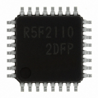
R5F21102DFP#U0 Renesas Electronics America, R5F21102DFP#U0 Datasheet - Page 125

R5F21102DFP#U0
Manufacturer Part Number
R5F21102DFP#U0
Description
IC R8C MCU FLASH 8K 32LQFP
Manufacturer
Renesas Electronics America
Series
M16C™ M16C/R8C/Tiny/10r
Datasheets
1.R5F211A2SPU0.pdf
(300 pages)
2.R5F21102FPU0.pdf
(30 pages)
3.R5F21102FPU0.pdf
(201 pages)
Specifications of R5F21102DFP#U0
Core Processor
R8C
Core Size
16-Bit
Speed
16MHz
Connectivity
SIO, UART/USART
Peripherals
LED, WDT
Number Of I /o
22
Program Memory Size
8KB (8K x 8)
Program Memory Type
FLASH
Ram Size
512 x 8
Voltage - Supply (vcc/vdd)
2.7 V ~ 5.5 V
Data Converters
A/D 8x10b
Oscillator Type
Internal
Operating Temperature
-40°C ~ 85°C
Package / Case
32-LQFP
For Use With
R0K521134S000BE - KIT EVAL STARTER FOR R8C/13R0E521134EPB00 - KIT EMULATOR PROBE FOR PC7501R0E521134CPE00 - EMULATOR COMPACT R8C/13
Lead Free Status / RoHS Status
Lead free / RoHS Compliant
Eeprom Size
-
Available stocks
Company
Part Number
Manufacturer
Quantity
Price
- Current page: 125 of 201
- Download datasheet (2Mb)
R8C/10 Group
Rev.1.20 Jan 27, 2006
REJ09B0019-0120
14.7 Output Impedance of Sensor under A/D Conversion
To carry out A/D conversion properly, charging the internal capacitor C shown in Figure 14.11 has to
be completed within a specified period of time. T (sampling time) as the specified time. Let output
impedance of sensor equivalent circuit be R0, microcomputer’s internal resistance be R, precision
(error) of the A/D converter be X, and the A/D converter’s resolution be Y (Y is 1024 in the 10-bit mode,
and 256 in the 8-bit mode).
Figure 14.11 shows analog input pin and external sensor equivalent circuit. When the difference
between VIN and VC becomes 0.1 LSB, we find impedance R0 when voltage between pins VC
changes from 0 to VIN – (0.1/1024) VIN in time T. (0.1/1024) means that A/D precision drop due to
insufficient capacitor charge is held to 0.1 LSB at time of A/D conversion in the 10-bit mode. Actual
error however is the value of absolute precision added to 0.1 LSB. When f(X
in the A/D conversion mode with sample & hold. Output impedance R0 for sufficiently charging capaci-
tor C within time T is determined as follows.
Thus, the allowable output impedance of the sensor circuit capable of thoroughly driving the A/D
converter turns out to be approximately 7.3 k .
R0 = –
VC is generally VC = VIN {1 – e
And when t = T,
Hence, R0 = –
T = 0.25 s, R = 2.8 k , C = 1.5 pF, X = 0.1, and Y = 1024 . Hence,
6.0 X 10
page 113 of 180
0.25 X 10
e
–
C • ln
–12
–
VC=VIN –
C (R0 +R)
• ln
C (R0 + R)
T
1
–6
1
X
Y
1024
0.1
– R
T
Y
X
T = ln
–
– 2.8 X 10
=
C (R0 + R)
VIN = VIN(1 –
1
Y
X
Y
X
14.7 Output Impedance of Sensor under A/D Conversion
3
t
}
7.3 X 10
Y
X
)
3
IN
) = 10 MHz, T = 0.25 µs
Related parts for R5F21102DFP#U0
Image
Part Number
Description
Manufacturer
Datasheet
Request
R

Part Number:
Description:
KIT STARTER FOR M16C/29
Manufacturer:
Renesas Electronics America
Datasheet:

Part Number:
Description:
KIT STARTER FOR R8C/2D
Manufacturer:
Renesas Electronics America
Datasheet:

Part Number:
Description:
R0K33062P STARTER KIT
Manufacturer:
Renesas Electronics America
Datasheet:

Part Number:
Description:
KIT STARTER FOR R8C/23 E8A
Manufacturer:
Renesas Electronics America
Datasheet:

Part Number:
Description:
KIT STARTER FOR R8C/25
Manufacturer:
Renesas Electronics America
Datasheet:

Part Number:
Description:
KIT STARTER H8S2456 SHARPE DSPLY
Manufacturer:
Renesas Electronics America
Datasheet:

Part Number:
Description:
KIT STARTER FOR R8C38C
Manufacturer:
Renesas Electronics America
Datasheet:

Part Number:
Description:
KIT STARTER FOR R8C35C
Manufacturer:
Renesas Electronics America
Datasheet:

Part Number:
Description:
KIT STARTER FOR R8CL3AC+LCD APPS
Manufacturer:
Renesas Electronics America
Datasheet:

Part Number:
Description:
KIT STARTER FOR RX610
Manufacturer:
Renesas Electronics America
Datasheet:

Part Number:
Description:
KIT STARTER FOR R32C/118
Manufacturer:
Renesas Electronics America
Datasheet:

Part Number:
Description:
KIT DEV RSK-R8C/26-29
Manufacturer:
Renesas Electronics America
Datasheet:

Part Number:
Description:
KIT STARTER FOR SH7124
Manufacturer:
Renesas Electronics America
Datasheet:

Part Number:
Description:
KIT STARTER FOR H8SX/1622
Manufacturer:
Renesas Electronics America
Datasheet:

Part Number:
Description:
KIT DEV FOR SH7203
Manufacturer:
Renesas Electronics America
Datasheet:


