R5F21102DFP#U0 Renesas Electronics America, R5F21102DFP#U0 Datasheet - Page 170
R5F21102DFP#U0
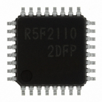
Manufacturer Part Number
R5F21102DFP#U0
Description
IC R8C MCU FLASH 8K 32LQFP
Manufacturer
Renesas Electronics America
Series
M16C™ M16C/R8C/Tiny/10r
Datasheets
1.R5F211A2SPU0.pdf
(300 pages)
2.R5F21102FPU0.pdf
(30 pages)
3.R5F21102FPU0.pdf
(201 pages)
Specifications of R5F21102DFP#U0
Core Processor
R8C
Core Size
16-Bit
Speed
16MHz
Connectivity
SIO, UART/USART
Peripherals
LED, WDT
Number Of I /o
22
Program Memory Size
8KB (8K x 8)
Program Memory Type
FLASH
Ram Size
512 x 8
Voltage - Supply (vcc/vdd)
2.7 V ~ 5.5 V
Data Converters
A/D 8x10b
Oscillator Type
Internal
Operating Temperature
-40°C ~ 85°C
Package / Case
32-LQFP
For Use With
R0K521134S000BE - KIT EVAL STARTER FOR R8C/13R0E521134EPB00 - KIT EMULATOR PROBE FOR PC7501R0E521134CPE00 - EMULATOR COMPACT R8C/13
Lead Free Status / RoHS Status
Lead free / RoHS Compliant
Eeprom Size
-
Available stocks
Company
Part Number
Manufacturer
Quantity
Price


R8C/10 Group
Rev.1.20 Jan 27, 2006
REJ09B0019-0120
Table 17.7 Pin Functions (Flash Memory Standard Serial I/O Mode)
P 4
V
IV
R E S E T
P 4
A V
V
P 0
P 1
P3
P 4
P 0
M O D E
C N V
P3
C C
R E F
CC
7
6
1
0
0
5
0
7
C C
/ X
/ X
, V
t o P 0
t o P 1
to P3
S S
, A V
I N
O U T
S S
P i n
7
7
3
S S
R e s e t i n p u t
P 4
P 4
A n a l o g p o w e r s u p p l y i n p u t
I n p u t p o r t P 0
I n p u t p o r t P 1
Input port P3
I n p u t p o r t P 4
T x D o u t p u t
M O D E
C N V
RxD input
R e f e r e n c e v o l t a g e i n p u t
P o w e r i n p u t
IV
6
7
page 158 of 180
CC
i n p u t / C l o c k i n p u t
i n p u t / C l o c k o u t p u t
S S
N a m e
I/O
I/O
I/O
I / O
I
I
I
I
I
I
I
O
I
I
Connect a ceramic resonator or crystal oscillator between X
X
mode 1, connect a ceramic resonator or crystal oscillator between X
not using the main clock in standard serial I/O mode 1, connect this pin to Vcc via a resistor
(pull-up).
A p p l y t h e v o l t a g e g u a r a n t e e d f o r P r o g r a m a n d E r a s e t o V c c p i n a n d
0 V t o V s s p i n .
Connect capacitor (0.1 µF) to Vss.
Reset input pin.
Connect AVss to Vss and AVcc to Vcc, respectively.
Enter the reference voltage for AD from this pin.
Input "H" or "L" level signal or open.
Input "H" or "L" level signal or open.
Input "H" or "L" level signal or open.
Input "H" or "L" level signal or open.
Serial data output pin
Standard serial I/O mode 1: connect to flash programmer
Standard serial I/O mode 2: Input "L".
Serial data input pin
S t a n d a r d s e r i a l I / O m o d e 1 : c o n n e c t t o f l a s h p r o g r a m m e r
S t a n d a r d s e r i a l I / O m o d e 2 : I n p u t " L " .
OUT
pins in standard serial I/O mode 2. When using the main clock in standard serial I/O
Description
17.5 Standard Serial I/O Mode
IN
and
IN
and X
OUT
pins. When
Related parts for R5F21102DFP#U0
Image
Part Number
Description
Manufacturer
Datasheet
Request
R

Part Number:
Description:
KIT STARTER FOR M16C/29
Manufacturer:
Renesas Electronics America
Datasheet:

Part Number:
Description:
KIT STARTER FOR R8C/2D
Manufacturer:
Renesas Electronics America
Datasheet:

Part Number:
Description:
R0K33062P STARTER KIT
Manufacturer:
Renesas Electronics America
Datasheet:

Part Number:
Description:
KIT STARTER FOR R8C/23 E8A
Manufacturer:
Renesas Electronics America
Datasheet:

Part Number:
Description:
KIT STARTER FOR R8C/25
Manufacturer:
Renesas Electronics America
Datasheet:

Part Number:
Description:
KIT STARTER H8S2456 SHARPE DSPLY
Manufacturer:
Renesas Electronics America
Datasheet:

Part Number:
Description:
KIT STARTER FOR R8C38C
Manufacturer:
Renesas Electronics America
Datasheet:

Part Number:
Description:
KIT STARTER FOR R8C35C
Manufacturer:
Renesas Electronics America
Datasheet:

Part Number:
Description:
KIT STARTER FOR R8CL3AC+LCD APPS
Manufacturer:
Renesas Electronics America
Datasheet:
Part Number:
Description:
KIT STARTER FOR RX610
Manufacturer:
Renesas Electronics America
Datasheet:

Part Number:
Description:
KIT STARTER FOR R32C/118
Manufacturer:
Renesas Electronics America
Datasheet:

Part Number:
Description:
KIT DEV RSK-R8C/26-29
Manufacturer:
Renesas Electronics America
Datasheet:

Part Number:
Description:
KIT STARTER FOR SH7124
Manufacturer:
Renesas Electronics America
Datasheet:

Part Number:
Description:
KIT STARTER FOR H8SX/1622
Manufacturer:
Renesas Electronics America
Datasheet:

Part Number:
Description:
KIT DEV FOR SH7203
Manufacturer:
Renesas Electronics America
Datasheet: