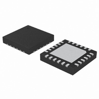
C8051F988-GM Silicon Laboratories Inc, C8051F988-GM Datasheet - Page 244

C8051F988-GM
Manufacturer Part Number
C8051F988-GM
Description
IC MCU 8BIT 4KB FLASH 24QFN
Manufacturer
Silicon Laboratories Inc
Series
C8051F9xxr
Specifications of C8051F988-GM
Program Memory Type
FLASH
Program Memory Size
4KB (4K x 8)
Package / Case
24-UQFN Exposed Pad, 24-HUQFN
Core Processor
8051
Core Size
8-Bit
Speed
25MHz
Connectivity
SMBus (2-Wire/I²C), SPI, UART/USART
Peripherals
Brown-out Detect/Reset, POR, PWM, Temp Sensor, WDT
Number Of I /o
17
Ram Size
512 x 8
Voltage - Supply (vcc/vdd)
1.8 V ~ 3.6 V
Data Converters
A/D 10x10b
Oscillator Type
Internal
Operating Temperature
-40°C ~ 85°C
Processor Series
C8051F9x
Core
8051
Data Ram Size
512 B
Interface Type
I2C, SMBus, Enhanced UART, Enhanced SPI
Maximum Clock Frequency
7 KHz
Number Of Programmable I/os
17
Number Of Timers
4
Operating Supply Voltage
2.4 V
Maximum Operating Temperature
+ 85 C
Mounting Style
SMD/SMT
3rd Party Development Tools
PK51, CA51, A51, ULINK2
Development Tools By Supplier
C8051F996DK
Minimum Operating Temperature
- 40 C
On-chip Adc
10 bit, 10 Channel
On-chip Dac
10 bit, 4 Channel
Lead Free Status / RoHS Status
Lead free / RoHS Compliant
Eeprom Size
-
Lead Free Status / Rohs Status
Lead free / RoHS Compliant
Other names
336-1959-5
- Current page: 244 of 322
- Download datasheet (3Mb)
C8051F99x-C8051F98x
22.4.3. Hardware Slave Address Recognition
The SMBus hardware has the capability to automatically recognize incoming slave addresses and send an
ACK without software intervention. Automatic slave address recognition is enabled by setting the EHACK
bit in register SMB0ADM to 1. This will enable both automatic slave address recognition and automatic
hardware ACK generation for received bytes (as a master or slave). More detail on automatic hardware
ACK generation can be found in Section 22.4.2.2.
The registers used to define which address(es) are recognized by the hardware are the SMBus Slave
Address register (SFR Definition 22.3) and the SMBus Slave Address Mask register (SFR Definition 22.4).
A single address or range of addresses (including the General Call Address 0x00) can be specified using
these two registers. The most-significant seven bits of the two registers are used to define which
addresses will be ACKed. A 1 in bit positions of the slave address mask SLVM[6:0] enable a comparison
between the received slave address and the hardware’s slave address SLV[6:0] for those bits. A 0 in a bit
of the slave address mask means that bit will be treated as a “don’t care” for comparison purposes. In this
case, either a 1 or a 0 value are acceptable on the incoming slave address. Additionally, if the GC bit in
register SMB0ADR is set to 1, hardware will recognize the General Call Address (0x00). Table 22.4 shows
some example parameter settings and the slave addresses that will be recognized by hardware under
those conditions.
244
Hardware Slave Address
SLV[6:0]
0x34
0x34
0x34
0x34
0x70
Table 22.4. Hardware Address Recognition Examples (EHACK = 1)
Slave Address Mask
SLVM[6:0]
0x7E
0x7E
0x7F
0x7F
0x73
Rev. 1.0
GC bit
0
1
0
1
0
Slave Addresses Recognized by
Hardware
0x34
0x34, 0x00 (General Call)
0x34, 0x35
0x34, 0x35, 0x00 (General Call)
0x70, 0x74, 0x78, 0x7C
Related parts for C8051F988-GM
Image
Part Number
Description
Manufacturer
Datasheet
Request
R
Part Number:
Description:
SMD/C°/SINGLE-ENDED OUTPUT SILICON OSCILLATOR
Manufacturer:
Silicon Laboratories Inc
Part Number:
Description:
Manufacturer:
Silicon Laboratories Inc
Datasheet:
Part Number:
Description:
N/A N/A/SI4010 AES KEYFOB DEMO WITH LCD RX
Manufacturer:
Silicon Laboratories Inc
Datasheet:
Part Number:
Description:
N/A N/A/SI4010 SIMPLIFIED KEY FOB DEMO WITH LED RX
Manufacturer:
Silicon Laboratories Inc
Datasheet:
Part Number:
Description:
N/A/-40 TO 85 OC/EZLINK MODULE; F930/4432 HIGH BAND (REV E/B1)
Manufacturer:
Silicon Laboratories Inc
Part Number:
Description:
EZLink Module; F930/4432 Low Band (rev e/B1)
Manufacturer:
Silicon Laboratories Inc
Part Number:
Description:
I°/4460 10 DBM RADIO TEST CARD 434 MHZ
Manufacturer:
Silicon Laboratories Inc
Part Number:
Description:
I°/4461 14 DBM RADIO TEST CARD 868 MHZ
Manufacturer:
Silicon Laboratories Inc
Part Number:
Description:
I°/4463 20 DBM RFSWITCH RADIO TEST CARD 460 MHZ
Manufacturer:
Silicon Laboratories Inc
Part Number:
Description:
I°/4463 20 DBM RADIO TEST CARD 868 MHZ
Manufacturer:
Silicon Laboratories Inc
Part Number:
Description:
I°/4463 27 DBM RADIO TEST CARD 868 MHZ
Manufacturer:
Silicon Laboratories Inc
Part Number:
Description:
I°/4463 SKYWORKS 30 DBM RADIO TEST CARD 915 MHZ
Manufacturer:
Silicon Laboratories Inc
Part Number:
Description:
N/A N/A/-40 TO 85 OC/4463 RFMD 30 DBM RADIO TEST CARD 915 MHZ
Manufacturer:
Silicon Laboratories Inc
Part Number:
Description:
I°/4463 20 DBM RADIO TEST CARD 169 MHZ
Manufacturer:
Silicon Laboratories Inc


