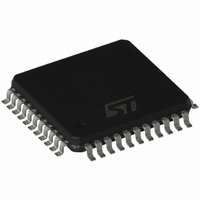
ST72F324BJ6T6 STMicroelectronics, ST72F324BJ6T6 Datasheet - Page 180

ST72F324BJ6T6
Manufacturer Part Number
ST72F324BJ6T6
Description
IC MCU 8BIT 32K FLASH 44-LQFP
Manufacturer
STMicroelectronics
Series
ST7r
Datasheet
1.ST72F324BJ2T6.pdf
(198 pages)
Specifications of ST72F324BJ6T6
Core Processor
ST7
Core Size
8-Bit
Speed
8MHz
Connectivity
SCI, SPI
Peripherals
LVD, POR, PWM, WDT
Number Of I /o
32
Program Memory Size
32KB (32K x 8)
Program Memory Type
FLASH
Ram Size
1K x 8
Voltage - Supply (vcc/vdd)
3.8 V ~ 5.5 V
Data Converters
A/D 12x10b
Oscillator Type
Internal
Operating Temperature
-40°C ~ 85°C
Package / Case
44-TQFP, 44-VQFP
Processor Series
ST72F3x
Core
ST7
Data Bus Width
8 bit
Data Ram Size
1 KB
Interface Type
SCI, SPI
Maximum Clock Frequency
8 MHz
Number Of Programmable I/os
32
Number Of Timers
3
Maximum Operating Temperature
+ 85 C
Mounting Style
SMD/SMT
Development Tools By Supplier
ST7232X-EVAL, ST7MDT20-DVP3, ST7MDT20J-EMU3, STX-RLINK
Minimum Operating Temperature
- 40 C
On-chip Adc
10 bit, 12 Channel
For Use With
497-6421 - BOARD EVAL DGTL BATT CHGR DESIGN497-5046 - KIT TOOL FOR ST7/UPSD/STR7 MCU
Lead Free Status / RoHS Status
Lead free / RoHS Compliant
Eeprom Size
-
Lead Free Status / Rohs Status
Details
Other names
497-5590
Available stocks
Company
Part Number
Manufacturer
Quantity
Price
Company:
Part Number:
ST72F324BJ6T6
Manufacturer:
ON
Quantity:
301
Company:
Part Number:
ST72F324BJ6T6
Manufacturer:
STMicroelectronics
Quantity:
10 000
Company:
Part Number:
ST72F324BJ6T6TR
Manufacturer:
STMicroelectronics
Quantity:
10 000
Device configuration and ordering information
180/198
Table 117. Option byte 0 bit description (continued)
Table 118. Option byte 1 bit description
OPT4:3
OPT2:1
OPT5:4
OPT5
OPT0
OPT7
OPT6
Bit
Bit
OSCTYPE[1:0]
FMP_R
VD[1:0]
Name
RSTC
Name
PKG1
-
-
Pin package selection bit
Reset clock cycle selection
Oscillator type
Reserved, must be kept at default value.
Voltage detection
Reserved, must be kept at default value
Flash memory readout protection
This option bit selects the package (see
Note: On the chip, each I/O port has eight pads. Pads that are not
bonded to external pins are in input pull-up configuration after reset.
The configuration of these pads must be kept at reset state to avoid
added current consumption.
This option bit selects the number of CPU cycles applied during the
reset phase and when exiting Halt mode. For resonator oscillators, it
is advised to select 4096 due to the long crystal stabilization time.
0: Reset phase with 4096 CPU cycles
1: Reset phase with 256 CPU cycles
These option bits select the ST7 main clock source type.
00: Clock source = Resonator oscillator
01: Reserved
10: Clock source = Internal RC oscillator
11: Clock source = External source
These option bits enable the voltage detection block (LVD and AVD)
with a selected threshold for the LVD and AVD.
00: Selected LVD = Highest threshold (V
01: Selected LVD = Medium threshold (V
10: Selected LVD = Lowest threshold (V
11: LVD and AVD off
Caution: If the medium or low thresholds are selected, the detection
may occur outside the specified operating voltage range. Below 3.8V,
device operation is not guaranteed. For details on the AVD and LVD
threshold levels refer to
Readout protection, when selected, provides a protection against
program memory content extraction and against write access to Flash
memory.
Erasing the option bytes when the FMP_R option is selected causes
the whole user memory to be erased first, afterwhich the device can
be reprogrammed. Refer to
Flash Programming Reference Manual for more details.
0: Readout protection enabled
1: Readout protection disabled
Doc ID13466 Rev 4
Section 12.4.1 on page
Section 4.3.1 on page 23
Function
Function
DD
Table
DD
DD
~3V).
~4V).
~3.5V).
119).
149.
ST72324B-Auto
and the ST7


