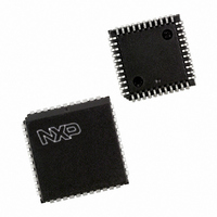
P87C591VFA/00,512 NXP Semiconductors, P87C591VFA/00,512 Datasheet - Page 73

P87C591VFA/00,512
Manufacturer Part Number
P87C591VFA/00,512
Description
IC 80C51 MCU 16K OTP 44-PLCC
Manufacturer
NXP Semiconductors
Series
87Cr
Datasheet
1.P87C591VFA00512.pdf
(160 pages)
Specifications of P87C591VFA/00,512
Core Processor
8051
Core Size
8-Bit
Speed
12MHz
Connectivity
CAN, EBI/EMI, I²C, UART/USART
Peripherals
POR, PWM, WDT
Number Of I /o
32
Program Memory Size
16KB (16K x 8)
Program Memory Type
OTP
Ram Size
512 x 8
Voltage - Supply (vcc/vdd)
4.75 V ~ 5.25 V
Data Converters
A/D 6x10b
Oscillator Type
Internal
Operating Temperature
-40°C ~ 85°C
Package / Case
44-PLCC
Processor Series
P87C5x
Core
80C51
Data Bus Width
8 bit
Data Ram Size
512 B
Interface Type
CAN, I2C, UART
Maximum Clock Frequency
12 MHz
Number Of Programmable I/os
32
Number Of Timers
3
Maximum Operating Temperature
+ 85 C
Mounting Style
SMD/SMT
3rd Party Development Tools
PK51, CA51, A51, ULINK2
Minimum Operating Temperature
- 40 C
On-chip Adc
10 bit, 6 Channel
Lead Free Status / RoHS Status
Lead free / RoHS Compliant
Eeprom Size
-
Lead Free Status / Rohs Status
Details
Other names
568-1256-5
935268182512
P87C591VFAA
935268182512
P87C591VFAA
Available stocks
Company
Part Number
Manufacturer
Quantity
Price
Company:
Part Number:
P87C591VFA/00,512
Manufacturer:
TI
Quantity:
8
Company:
Part Number:
P87C591VFA/00,512
Manufacturer:
NXP Semiconductors
Quantity:
10 000
Philips Semiconductors
Mode 0 is the Shift Register mode and SM2 is ignored.
Using the Automatic Address Recognition feature allows a
master to selectively communicate with one or more
slaves by invoking the Given slave address or addresses.
All of the slaves may be contacted by using the Broadcast
address. All of the slaves may be contacted by using the
Broadcast address. Two Special Function Registers are
used to define the slave’s address, SADDR, and the
address mask, SADEN. SADEN is used to define which
bits in the SADDR are to be used and which bits are “don’t
care”. The SADEN mask can be logically ANDed with the
SADDR to create the “Given” address which the master
will use for addressing each of the slaves. Use of the Given
address allows multiple slaves to be recognized while
excluding others. The following examples will help to show
the versatility of this scheme:
In the above example SADDR is the same and the SADEN
data is used to differentiate between the two salves. Slave
0 requires as 0 in bit 0 and it ignores bit 1. Slave 1 requires
a 0 in bit 1 and bit 0 is ignored. A unique address for Slave
0 would be 1100 0010 since slave 1 requires a 0 in bit 1. A
unique address for Slave 1 would be 1100 0001 since a 1
in bit 0 will exclude slave 0. Both slaves can be selected at
the same time by an address which has bit 0 = 0 (for Slave
0) and bit 1 = 0 (for Slave 1). Thus, both could be
addressed with 1100 0000.
In a more complex system the following could be used to
select Slaves 1 and 2 while excluding Slave 0:
2000 Jul 26
Slave 0
Slave 1
Slave 0
Slave 1
Slave 2
Single-chip 8-bit microcontroller with CAN controller
SADDR =
SADEN =
Given
SADDR =
SADEN =
Given
SADDR =
SADEN =
Given
SADDR =
SADEN =
Given
SADDR =
SADEN =
Given
=
=
=
=
=
1100 0000
1111 1101
1100 00X0
1100 0000
1111 1110
1100 000X
1100 0000
1111 1001
1100 0XX0
1110 0000
1111 1010
1110 0X0X
1110 0000
1111 1100
1110 00XX
73
In the above example the differentiation among the 3
Slaves is in the lower 3 address bits. Slave 0 requires that
bit 0 = 0 and it can be uniquely addressed by 1110 0110.
Slave 1 requires that bit 1 = 0 and it can be uniquely
addressed by 1110 and 0101. Slave 2 requires that bit 2 =
0 and its unique address is 1110 0011. To select Slaves 0
and 1 and exclude Slave 2 use address 1110 0100, since
it is necessary to make bit 2 = 1 to exclude Slave 2.
The Broadcast Address for each slave is created by taking
the logical OR of SADDR and SADEN. Zeros in this result
are trended as don’t cares. In most cases, interpreting the
don’t-cares as ones, the broadcast address will be FF
hexadecimal.
Upon reset SADDR (SFR address 0A9H) and SADEN
(SFR address 0B9H) are leaded with 0s. This produces a
given address of all “don’t cares” as well as a Broadcast
address of all “don’t cares”. This effectively disables the
Automatic Addressing mode and allows the
microcontroller to use standard 80C51 type UART drivers
which do not make use of this feature.
15 SIO1, I
The I
information between devices connected to the bus. The
main features of the bus are:
The I/O pins P1.6 and P1.7 must be set to Open Drain
(SCL and SDA).
The 8xC591 on-chip I
that meets the I
handles bytes transfer autonomously. It also keeps track
of serial transfers, and a status register (S1STA) reflects
the status of SIO1 and the I
Bidirectional data transfer between masters and slaves
Multimaster bus (no central master)
Arbitration between simultaneously transmitting
masters without corruption of serial data on the bus
Serial clock synchronization allows devices with
different bit rates to communicate via one serial bus
Serial clock synchronization can be used as a
handshake mechanism to suspend and resume serial
transfer
The I
purposes
2
C bus uses two wires (SDA and SCL) to transfer
2
C bus may be used for test and diagnostic
2
C SERIAL IO
2
C bus specification. The SIO1 logic
2
C logic provides a serial interface
2
C bus.
Preliminary Specification
P8xC591


